In advanced electronics manufacturing, a circuit board purification project represents the critical infrastructure that determines yield, reliability, and long-term performance of printed circuit boards (PCBs) and electronic assemblies. With over two decades of experience designing cleanroom environments for semiconductor fabs, SMT lines, and PCB fabrication facilities, I have observed that improperly executed contamination control projects contribute to 15–25% of field failures—manifesting as ionic migration, solderability issues, and electrochemical corrosion. This technical guide dissects the engineering principles that define successful circuit board purification projects, from airborne molecular contamination (AMC) control to electrostatic discharge (ESD) mitigation and process-specific cleanliness protocols.
1. Contamination Sources in PCB Manufacturing: A Systematic Taxonomy
Effective circuit board purification projects begin with identifying the primary contamination vectors that threaten product quality:
Particulate contamination: Dust, fiber, and metallic particles from ambient air, personnel movement, and equipment wear. Particles >5 µm can cause solder mask voids; particles <0.5 µm can embed in surface finishes, leading to intermittent electrical failures.
Ionic contamination: Residual flux activators, process chemicals, and airborne salts (chlorides, sulfates) that promote electrochemical migration (ECM) and dendritic growth. Acceptable limits per IPC-5704: ≤1.56 µg NaCl eq/cm² for Class 3 assemblies.
Airborne molecular contamination (AMC): Organic compounds (outgassing from adhesives, lubricants) and acid gases (SO₂, NOx) that corrode copper traces and degrade solderability.
Electrostatic discharge (ESD): Static charge accumulation that damages sensitive components, with latent failures often undetected until field deployment.
Humidity-related issues: Moisture absorption leading to popcorning during reflow, and flux degradation affecting wetting.
A comprehensive purification project must address all five vectors through integrated cleanroom design, HVAC filtration, material selection, and process controls.
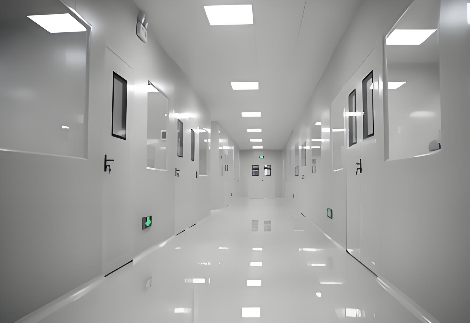
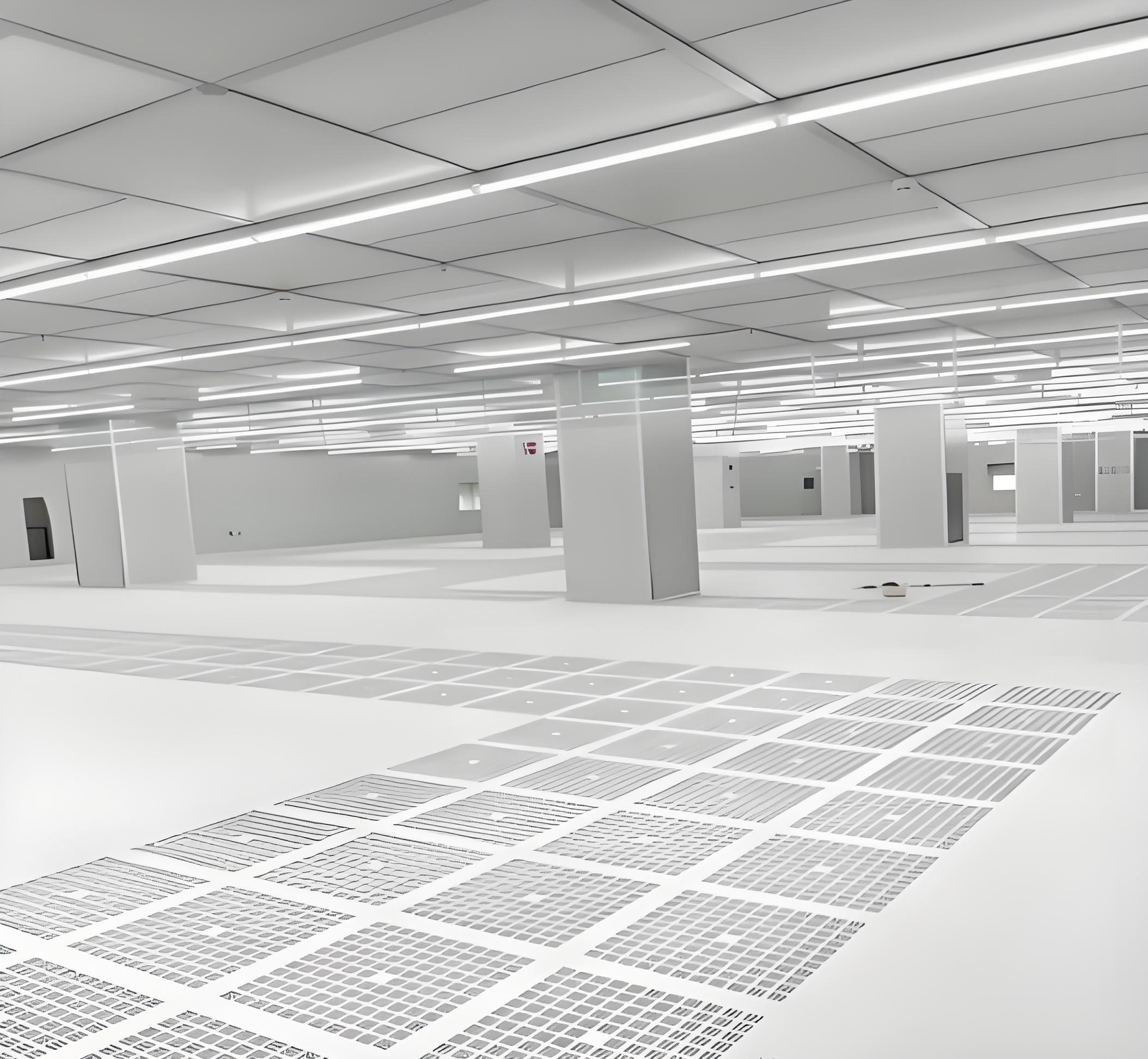
2. Cleanroom Classification: Matching ISO Class to Process Sensitivity
The cleanroom classification for a circuit board purification project is determined by the most sensitive process step:
ISO Class 5 (Class 100): Required for semiconductor wafer fabrication, fine-pitch component assembly (<0.3 mm pitch), and advanced packaging (flip-chip, 3D integration). Particle count limit: 3,520 particles ≥0.5 µm per m³.
ISO Class 6 (Class 1,000): Typical for SMT assembly lines, BGA rework, and conformal coating applications. Limits: 35,200 particles ≥0.5 µm per m³.
ISO Class 7 (Class 10,000): Suitable for PCB fabrication (etching, lamination), wave soldering, and general assembly areas. Limits: 352,000 particles ≥0.5 µm per m³.
ISO Class 8 (Class 100,000): For warehousing, shipping/receiving, and support areas with less stringent cleanliness requirements.
Hybrid facilities often employ zoning strategies: critical zones (solder paste printing, underfill dispensing) maintained at ISO 5–6, while less sensitive areas operate at ISO 7–8. This approach reduces construction and operating costs by 30–40% compared to single-class facilities.
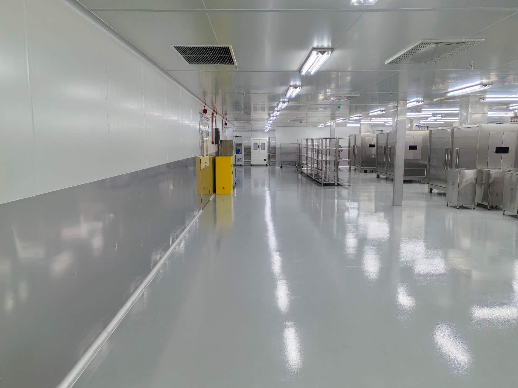
3. HVAC and Filtration Architecture
The air handling system is the mechanical heart of any circuit board purification project. Critical specifications:
HEPA/ULPA filtration: HEPA filters (99.97% at 0.3 µm) for ISO 7–8; ULPA filters (99.9995% at 0.12 µm) for ISO 5–6. Filter housing must be leak-tested per IEST-RP-CC034.2, with ≤0.01% penetration.
Chemical filtration: Activated carbon filters for organic vapors; impregnated chemisorption media (potassium permanganate, impregnated alumina) for acid gases and amines. Media bed depth: 50–100 mm for general AMC control; 150–300 mm for high-sensitivity zones.
Air change rates: ISO 5: 400–600 air changes per hour (ACH); ISO 6: 150–250 ACH; ISO 7: 60–90 ACH; ISO 8: 20–40 ACH. These rates ensure contaminant dilution and laminar flow maintenance.
Laminar vs. turbulent flow: ISO 5 requires unidirectional laminar flow (0.45 m/s ±20%) to sweep particles away from work surfaces. Lower classes can utilize turbulent (mixed) flow with strategic return air placements.
Energy recovery wheels (enthalpy wheels) can reduce HVAC energy consumption by 20–35% by preconditioning fresh air with exhaust air, essential for facilities in extreme climates.
4. Airborne Molecular Contamination (AMC) Control
AMC is increasingly recognized as a dominant yield killer in advanced electronics. A robust circuit board purification project must specify:
AMC monitoring: Real-time ion mobility spectrometry (IMS) for acids and bases; thermal desorption GC-MS for organics. Target levels per SEMI F21-1102: <5 ppb for acids (HF, HCl, H₂SO₄), <10 ppb for bases (NH₃, amines), <20 ppb for condensable organics.
Material selection: Low-outgassing materials (per ASTM E595) for all cleanroom furnishings, sealants, and packaging. PVC and certain adhesives are prohibited in high-sensitivity zones.
Process exhaust isolation: Soldering, flux application, and chemical processes must have dedicated exhaust systems with separate filtration to prevent cross-contamination of cleanroom air.
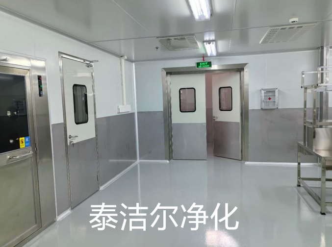
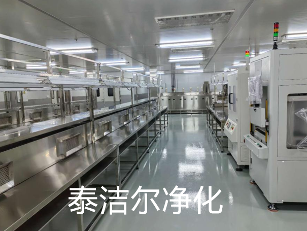
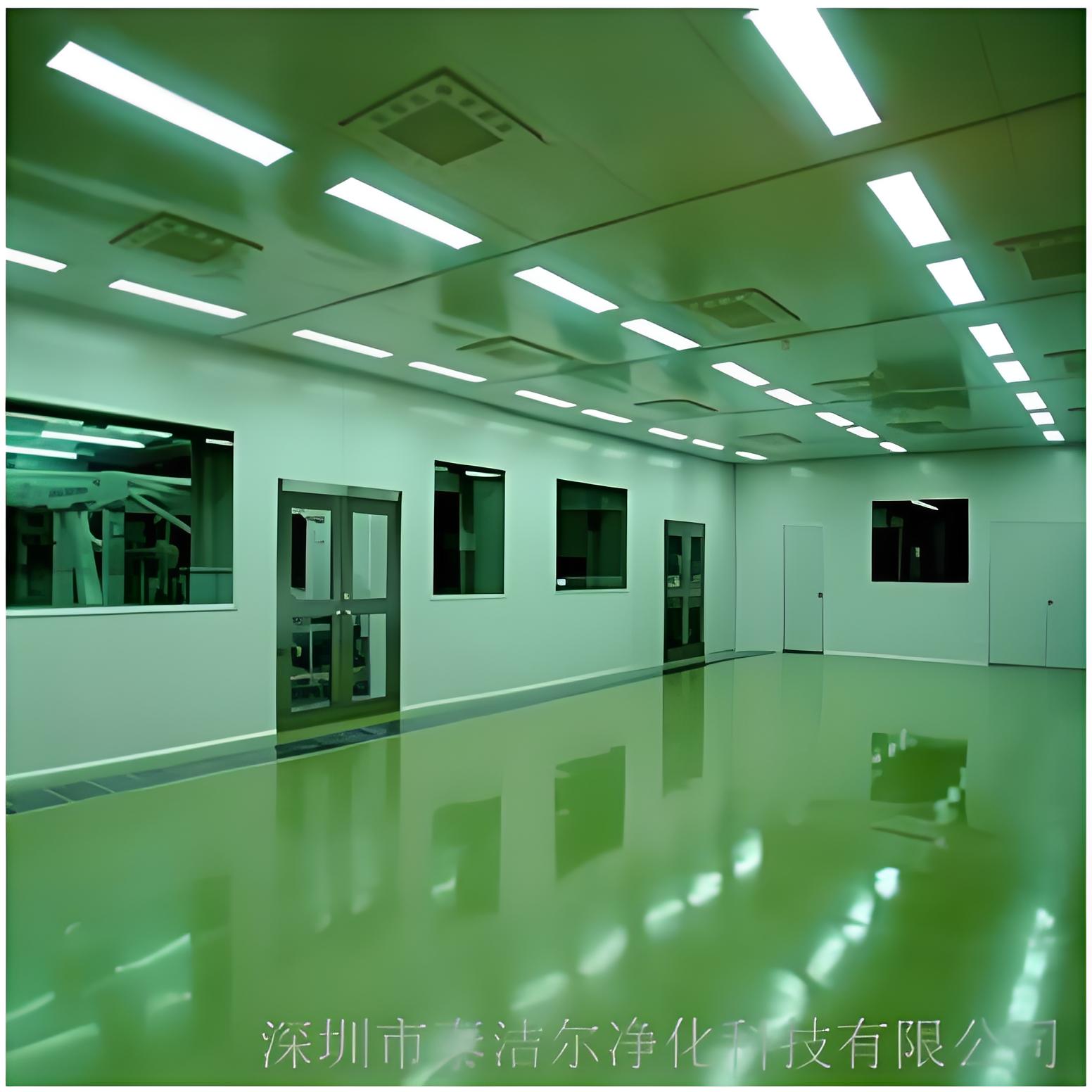
Leading integrators like TAI JIE ER provide turnkey AMC control systems incorporating real-time monitoring, adaptive filtration, and predictive maintenance alerts to maintain strict chemical purity.
5. Electrostatic Discharge (ESD) Protection Integration
ESD events cause immediate and latent damage to electronic components. A comprehensive circuit board purification project incorporates:
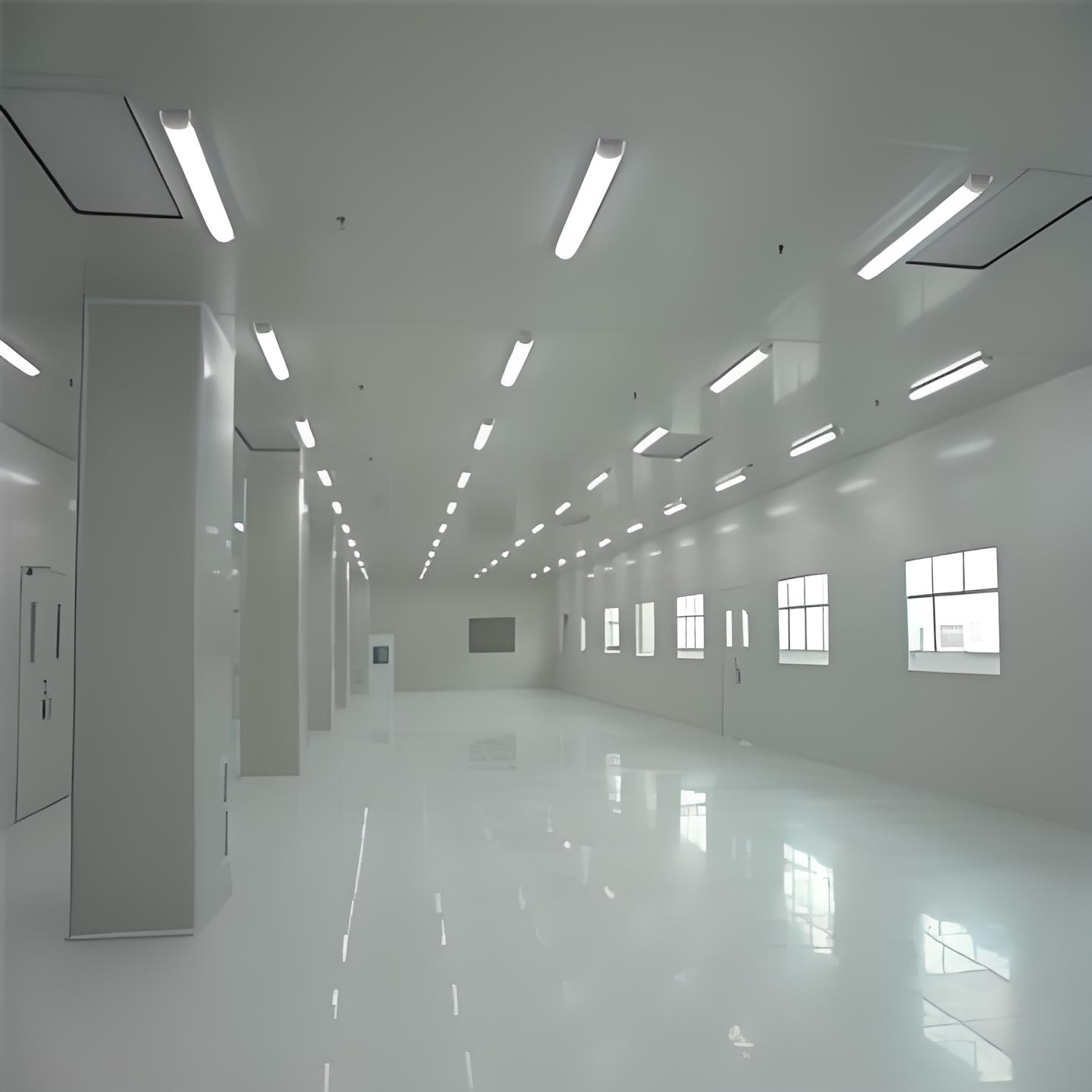
Conductive flooring: Epoxy terrazzo or vinyl tile with surface resistivity 10⁵–10⁹ ohms/sq, grounded via copper grid with <1 ohm resistance to facility ground. Static-dissipative coatings with <100V triboelectric charge generation.
ESD-safe work surfaces: Laminates with embedded conductive layer, connected to ground via 1 MΩ resistor chains. Workstations equipped with continuous monitors that alert operators when ground path resistance exceeds specifications.
Ionization systems: Overhead or benchtop ionizers neutralize static charges on insulators (plastic carriers, component trays). Balance specification: ±50V max, with decay time <2 seconds at 1,000V to 100V.
Personnel grounding: Wrist straps (with 1 MΩ resistor) and ESD footwear testers at entry points. Garments must incorporate conductive fibers with <10⁸ ohms/sq surface resistivity.
ESD audits per ANSI/ESD S20.20 should verify all elements quarterly; non-compliance accounts for 35% of unexplained field failures in sensitive electronics.
6. Process-Specific Purification Strategies
Different manufacturing stages impose unique cleanliness requirements:
Solder paste printing: ISO 5–6 environment with temperature 22–26°C ±1°C, RH 40–60%. Airborne particles >0.5 µm must be minimized to prevent stencil clogging and paste contamination.
Reflow soldering: Nitrogen atmosphere (O₂ <50 ppm) reduces oxidation and improves wetting. Exhaust systems must capture flux volatiles before they condense on equipment or re-enter cleanroom.
Conformal coating and underfill: ISO 5–7 with strict AMC control (organics <20 ppb). Coating voids caused by particle contamination can lead to moisture ingress and corrosion.
PCB fabrication (etching, plating): ISO 7–8 with segregated wet process areas. Acid-resistant materials for walls, floors, and ductwork to withstand chemical exposure.
Inspection and test: ISO 6–7 with anti-vibration flooring for automated optical inspection (AOI) and X-ray systems to maintain measurement accuracy.
Flexible cleanroom layouts with modular wall systems allow reconfiguration as processes evolve, reducing future capital expenditure by 40–60%.
7. Cleanroom Consumables and Hygiene Protocols
Personnel remain the largest contamination source. Effective protocols include:
Garmenting: ISO 5–6: full bunny suits with hood, face mask, gloves, and boot covers. ISO 7–8: frocks, hairnets, and dedicated footwear. Garment change frequency: 4–8 hours for high-class areas.
Sticky mats and air showers: 5-step sticky mats at entrances remove 90% of sole particles. Air showers (25–30 m/s velocity) dislodge loose particles from garments before cleanroom entry.
Cleaning materials: 100% continuous filament polyester wipers (non-linting) with IPA or DI water. Mop systems with microfiber pads and HEPA-filtered vacuums for floor cleaning.
Chemical compatibility: All cleaning agents must be validated for no residue and no reaction with process materials. Ionic contamination from cleaning agents is a common hidden defect source.
Training programs should include contamination awareness, proper gowning technique, and protocol enforcement—documented in ISO 14644-5 cleanroom operation standards.
8. Validation, Monitoring, and Continuous Improvement
Post-construction, a circuit board purification project requires rigorous qualification and ongoing monitoring:
ISO 14644 certification: Includes particle count testing at rest and operational states, air change rate verification, and filter leak testing. Re-certification intervals: 6–12 months.
Ionic contamination testing: Omegameter or ion chromatography testing of process boards per IPC-TM-650 2.3.28. Acceptance criteria based on product class (Class 1, 2, 3).
Surface insulation resistance (SIR) monitoring: Continuous measurement of comb pattern coupons identifies flux residue-related ECM risks. SIR values >10⁸ ohms required post-assembly.
Real-time monitoring: Networked particle counters, temperature/humidity sensors, and AMC analyzers provide alarm notifications and trend analysis. Data integration into manufacturing execution systems (MES) enables closed-loop process adjustments.
Data-driven facilities achieve 20–30% higher first-pass yields compared to those relying on periodic manual testing alone.
9. Turnkey Project Execution and Supplier Qualifications
Executing a successful circuit board purification project requires a supplier with cross-disciplinary expertise:
Cleanroom design-build: Architectural, mechanical, electrical, and process integration under single responsibility reduces coordination risks and schedule delays.
Pre-construction simulation: Computational fluid dynamics (CFD) modeling validates airflow patterns, temperature distribution, and contaminant removal before construction begins.
Modular construction: Prefabricated wall panels, ceiling grids, and mechanical skids accelerate installation by 30–50% compared to site-built construction.
Qualified commissioning: Independent third-party testing and documentation packages support regulatory compliance and insurance requirements.
TAI JIE ER specializes in turnkey cleanroom solutions for electronics manufacturing, with integrated project management from conceptual design through operational handover, ensuring alignment with production schedules and quality targets.
Frequently Asked Questions (FAQ)
Q1: What is the typical timeline for implementing a circuit board purification project for a new SMT line?
A1: For a standard SMT line cleanroom of 200–500 m², timeline typically spans 16–24 weeks: 2–4 weeks for concept design and engineering; 6–8 weeks for modular cleanroom fabrication; 4–6 weeks for on-site installation (including HVAC, electrical, and process utilities); and 2–4 weeks for commissioning, certification, and training. Expedited projects using pre-engineered systems can reduce total duration to 12–14 weeks.
Q2: How do I determine the required ISO class for my circuit board assembly operations?
A2: Classification is based on the most sensitive component
pitch and process. Guidelines:
— Component pitch >0.5 mm: ISO 8 (Class
100,000) sufficient.
— Pitch 0.3–0.5 mm or BGA/CSP: ISO 7 (Class 10,000)
recommended.
— Pitch <0.3 mm, flip-chip, or 01005 passives: ISO 6 (Class
1,000) minimum.
— Wafer-level packaging, 3D integration: ISO 5 (Class
100).
IPC-9801 provides detailed correlation between cleanliness levels and
defect rates.
Q3: What are the most common failure modes in circuit board purification projects?
A3: Top failure modes include:
(1) Inadequate AMC
filtration leading to corrosion of fine-pitch copper traces.
(2) Improper
cleanroom pressurization causing contamination infiltration from adjacent
areas.
(3) Insufficient ESD flooring continuity resulting in latent component
damage.
(4) Over-specified HVAC systems causing humidity fluctuations
(condensation risk).
(5) Lack of proper gowning protocols undermining
cleanroom investment.
Preventive measures include rigorous FAT/SAT testing
and operator training programs.
Q4: How does a circuit board purification project impact operational costs?
A4: While initial capital costs range from $2,500–$5,000 per
m² for cleanroom construction (depending on classification), operational
benefits typically include:
— Yield improvement: 5–15% reduction in defects,
increasing throughput without additional capital.
— Reduced rework costs:
lower labor and material waste.
— Extended equipment life: less
contamination-related wear on placement machines and soldering equipment.
—
Customer compliance: ability to qualify for high-reliability markets
(automotive, medical, aerospace).
Most facilities achieve payback within
12–24 months through yield gains alone.
Q5: Can an existing facility be retrofitted for higher cleanliness standards without production interruption?
A5: Yes, through phased retrofit strategies:
— Modular
cleanroom enclosures can be installed within existing buildings during
off-shifts or planned shutdowns.
— Temporary clean tents can maintain
production while permanent infrastructure is built adjacent.
— HVAC upgrades
can be staged, with portable filtration units supplementing during
transitions.
— Critical process zones can be upgraded first (e.g., solder
paste printing), followed by support areas.
Experienced integrators like
TAI JIE ER specialize in
low-disruption retrofits with detailed migration plans.
Q6: What certifications are required for suppliers of circuit board purification projects?
A6: Look for:
— ISO 9001:2015 (quality management).
—
Cleanroom construction experience with documented references in
electronics.
— In-house engineering capabilities (mechanical, electrical,
process).
— Ability to provide ISO 14644 certification testing.
— For AMC
control, suppliers should demonstrate expertise in chemical filtration media
selection and real-time monitoring systems.
— Turnkey providers should offer
single-point warranty coverage for all integrated systems.
Q7: How is a circuit board purification project validated for regulatory compliance?
A7: Validation packages typically include:
— IQ
(Installation Qualification): verification of materials, utilities, and as-built
drawings.
— OQ (Operational Qualification): testing of alarm systems, airflow
velocity, particle counts at rest, and HVAC control stability.
— PQ
(Performance Qualification): operational state testing with simulated production
loads, including particle count mapping, temperature/humidity uniformity, and
AMC sampling.
— Ongoing monitoring protocols with statistical process control
(SPC) charts to demonstrate continued compliance. Documentation follows GAMP 5
guidelines for automated systems and 21 CFR Part 11 where electronic records are
required.
For detailed engineering consultations, feasibility studies, or turnkey execution of your circuit board purification project, contact the cleanroom engineering team at TAI JIE ER—specialists in high-purity manufacturing environments for the global electronics industry.