In the semiconductor and electronics industries, electronic purification engineering represents the foundational discipline that transforms standard manufacturing spaces into high-yield, contamination-controlled environments. With over 25 years of experience designing cleanroom facilities for semiconductor fabs, PCB assembly lines, and precision optics manufacturers, I have observed that suboptimal purification strategies contribute to 18–30% of yield losses—manifesting as particulate-induced defects, ionic migration failures, and electrostatic discharge (ESD) damage. This technical guide dissects the engineering principles that define world-class electronic purification engineering, from airborne molecular contamination (AMC) control to vibration isolation and automated monitoring systems.
1. Contamination Vectors in Electronics Manufacturing: A Holistic Taxonomy
Effective electronic purification engineering addresses five primary contamination sources that compromise product quality:
Particulate contamination: Airborne dust, fibers, and metallic particles generated by personnel, equipment, and facility materials. Particles ≥0.5 µm can cause solder mask voids; particles ≤0.1 µm can embed in gate oxides, causing latent device failures.
Airborne molecular contamination (AMC): Acid gases (SO₂, NOx, HF), bases (NH₃, amines), and condensable organics that corrode copper traces, degrade solderability, and alter photoresist properties. SEMI F21-1102 specifies target levels: <5 ppb for acids, <10 ppb for bases.
Ionic contamination: Residual flux activators, processing chemicals, and airborne salts that promote electrochemical migration (ECM) and dendritic growth. IPC-5704 sets maximum limits at 1.56 µg NaCl eq/cm² for Class 3 assemblies.
Electrostatic discharge (ESD): Static charge accumulation causing immediate or latent damage to sensitive components. Devices with <100V sensitivity require stringent ESD controls per ANSI/ESD S20.20.
Vibration and mechanical disturbance: Equipment-generated vibrations that affect alignment in photolithography, wire bonding, and automated optical inspection (AOI). Vibration criteria (VC) curves define allowable levels for different process sensitivities.
A comprehensive purification project must integrate controls for all five vectors simultaneously, as interactions between contaminants (e.g., particles carrying ionic residues) compound defect mechanisms.
2. Cleanroom Classification and ISO 14644 Standards
The cornerstone of electronic purification engineering is selecting the appropriate ISO 14644-1 cleanroom class based on process sensitivity:
ISO Class 3 (Class 1): For advanced semiconductor lithography (≤7nm nodes), requiring <1,000 particles ≥0.1 µm per m³. Unidirectional laminar flow at 0.45 m/s ±20%.
ISO Class 4 (Class 10): For wafer fabrication, mask shops, and certain MEMS processes. Limits: 10,000 particles ≥0.1 µm per m³.
ISO Class 5 (Class 100): For photolithography steppers, inspection tools, and advanced packaging. Limits: 3,520 particles ≥0.5 µm per m³.
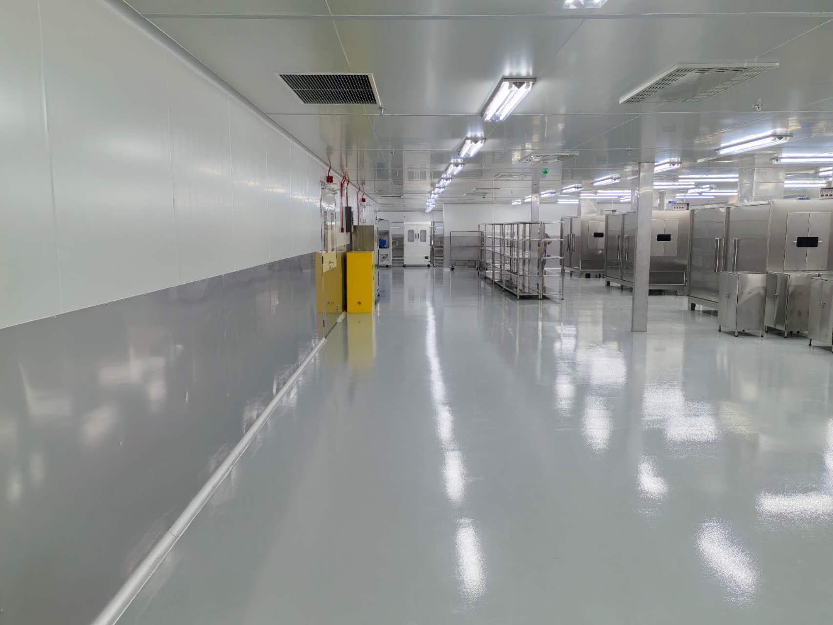
ISO Class 6 (Class 1,000): Typical for SMT assembly lines, BGA rework, and conformal coating. Limits: 35,200 particles ≥0.5 µm per m³.
ISO Class 7 (Class 10,000): For PCB fabrication, wave soldering, and general assembly. Limits: 352,000 particles ≥0.5 µm per m³.
ISO Class 8 (Class 100,000): For support areas, warehousing, and shipping/receiving.
Hybrid facilities often employ zoning: critical zones (e.g., solder paste printing) maintained at ISO 5–6, while less sensitive operations at ISO 7–8 reduce construction and operating costs by 25–35%.
3. HVAC and Filtration System Architecture
The mechanical core of electronic purification engineering is the air handling system. Critical specifications include:
HEPA/ULPA filtration: HEPA filters (99.97% at 0.3 µm) for ISO 7–8; ULPA filters (99.9995% at 0.12 µm) for ISO 5–6. Filter housing leak testing per IEST-RP-CC034.2 must show ≤0.01% penetration.
Chemical filtration: Activated carbon for organic vapors; impregnated chemisorption media (potassium permanganate, alumina) for acid gases and amines. Media bed depth: 50–150 mm depending on AMC load.
Air change rates (ACH): ISO 5: 400–600 ACH; ISO 6: 150–250 ACH; ISO 7: 60–90 ACH; ISO 8: 20–40 ACH. Higher rates improve contaminant dilution but increase energy consumption.
Airflow uniformity: For unidirectional zones, velocity variation ≤20% across the filter face. Computational fluid dynamics (CFD) modeling validates airflow patterns before construction.
Energy recovery wheels (enthalpy wheels) can reduce HVAC energy consumption by 20–35%—critical for large-scale facilities where cleanroom HVAC represents 40–50% of total energy use.
4. Airborne Molecular Contamination (AMC) Control Strategies
For advanced nodes and sensitive assembly, AMC control is a defining feature of modern electronic purification engineering:
Real-time AMC monitoring: Ion mobility spectrometry (IMS) for acids/bases; thermal desorption GC-MS for organics. Data integrated into facility monitoring systems with automated alerts.
Source control: Low-outgassing materials (ASTM E595) for all cleanroom furnishings, sealants, and consumables. PVC, certain adhesives, and silicone-based lubricants prohibited in high-sensitivity zones.
Process exhaust isolation: Soldering, flux application, and chemical processes have dedicated exhaust with separate chemical filtration to prevent cross-contamination of cleanroom recirculated air.
Pressure cascades: Positive pressure differentials (0.02–0.05 inches H₂O) between clean zones and adjacent areas prevent infiltration of contaminated air. Continuous monitoring with alarming.
Leading integrators like TAI JIE ER provide turnkey AMC management systems, including media selection, monitoring instrumentation, and adaptive control logic.
5. Electrostatic Discharge (ESD) Protection Infrastructure
ESD control is integral to electronic purification engineering, particularly for facilities handling sensitive components:
Conductive flooring: Epoxy or vinyl tile with surface resistivity 10⁵–10⁹ ohms/sq, grounded via copper grid with <1 ohm resistance to facility ground. Static-dissipative coatings with <100V triboelectric charge generation.
ESD-safe work surfaces: Laminates with embedded conductive layer, connected to ground via 1 MΩ resistor chains. Continuous monitors verify ground integrity.
Ionization systems: Overhead or benchtop ionizers neutralize static charges on insulators. Balance: ±50V max; decay time <2 seconds (1,000V to 100V).
Personnel grounding: Wrist straps (1 MΩ resistor), ESD footwear testers at entry, and conductive garments (surface resistivity <10⁸ ohms/sq).
Regular audits per ANSI/ESD S20.20 are mandatory; facilities lacking proper ESD controls report 25–40% higher field failure rates.
6. Vibration Isolation and Structural Dynamics
Precision manufacturing processes require vibration control. Electronic purification engineering must specify:
Vibration criteria (VC) curves: VC-A (50 µm/s) for manual assembly; VC-B (25 µm/s) for standard SMT; VC-C (12.5 µm/s) for fine-pitch placement; VC-D (6.25 µm/s) for photolithography; VC-E (3.12 µm/s) for advanced lithography and electron microscopy.
Structural design: Thickened concrete slabs (300–450 mm) with isolation joints separating cleanroom slab from building columns. Equipment-specific active vibration isolation systems for sensitive tools (e.g., wafer steppers).
Ambient vibration sources: HVAC equipment, pumps, and compressors mounted on inertia bases with spring isolators; utility lines routed through flexible connections to prevent transmission to cleanroom structure.
Pre-construction site surveys using seismographs establish baseline vibration levels; post-construction verification ensures criteria met.
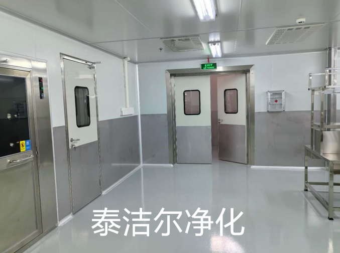
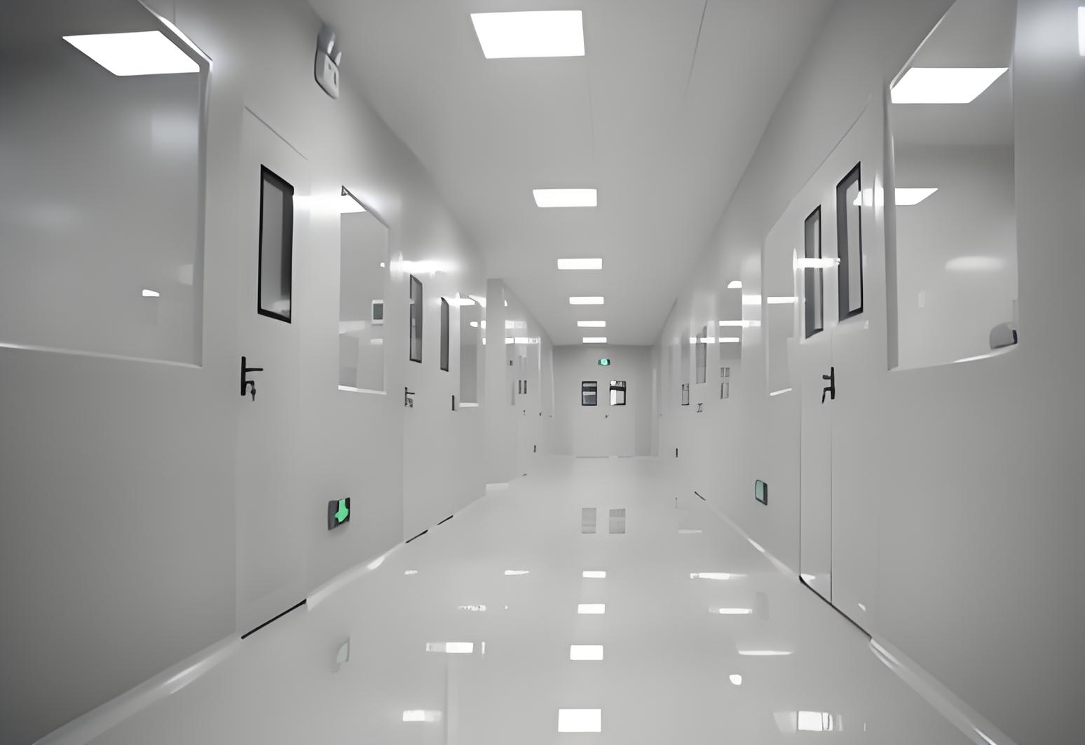
7. Material Selection and Cleanroom Compatibility
All materials within the clean envelope must be selected for minimal contamination generation:
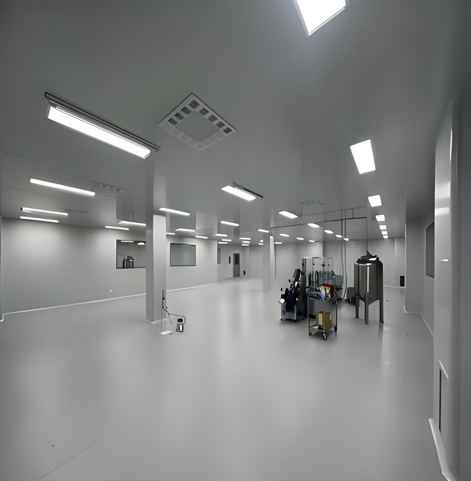
Wall and ceiling systems: Modular panels with smooth, non-porous surfaces (PVC-coated steel, aluminum with powder coating). Seams sealed with silicone-free, low-outgassing sealants.
Flooring: Seamless epoxy or polyurethane systems; sheet vinyl with welded seams. Surface hardness >85 Shore D to resist abrasion.
Lighting: Recessed LED fixtures with smooth lenses; no exposed fasteners. Fixtures sealed to ceiling grid.
Process equipment: Stainless steel (304/316L) with electropolished surfaces; internal cabling and components rated for cleanroom use (low particle emission).
Material selection documentation (certificates of conformance) must be maintained for regulatory audits (ISO 14644, SEMI S2).
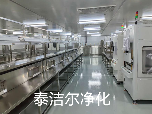
8. Process-Specific Purification Configurations
Different electronics manufacturing stages require tailored purification strategies:
Semiconductor wafer fab: ISO 3–5 with minienvironments around tools; stringent AMC control (sub-ppb); continuous vibration monitoring; advanced ESD controls including wafer handling automation.
SMT assembly: ISO 6–7 with zone-specific controls: solder paste printing at ISO 5–6; reflow zones with nitrogen atmosphere; AOI areas with anti-vibration flooring.
PCB fabrication: ISO 7–8 with segregated wet process areas; acid-resistant materials; dedicated exhaust for etching and plating lines.
Medical electronics: ISO 6–7 with emphasis on ionic cleanliness and biocompatibility; cleanroom garmenting protocols for Class III device manufacturing.
Automotive electronics: ISO 7–8 with focus on long-term reliability testing; thermal cycling chambers integrated into cleanroom envelope.
Flexible modular cleanroom designs allow reconfiguration as product mixes evolve, reducing future capital expenditure by 40–60%.
9. Monitoring, Automation, and Industry 4.0 Integration
Modern electronic purification engineering incorporates continuous monitoring and data analytics:
Real-time particle monitoring: Networked airborne particle counters (0.1–5.0 µm) with data logged to central historian. Alarms triggered when limits exceeded.
Environmental sensors: Temperature (±0.1°C), humidity (±1% RH), differential pressure, and vibration sensors integrated into building management system (BMS).
AMC monitoring: Ion mobility spectrometers and gas chromatography systems provide real-time AMC data; predictive algorithms optimize chemical filter change-out schedules.
ESD monitoring: Continuous wrist strap and workstation monitors; environmental ESD event counters.
Data integration: All monitoring data fed into manufacturing execution system (MES) for correlation with product quality metrics, enabling closed-loop process adjustments.
Facilities with comprehensive monitoring achieve 15–25% higher yields through rapid detection and correction of contamination excursions.
10. Lifecycle Cost Management and Sustainability
Total cost of ownership for electronic purification engineering extends beyond initial construction. Key considerations:
Energy efficiency: VFD-controlled fans, enthalpy wheels, and demand-controlled ventilation reduce annual energy costs by 20–35%.
Maintenance planning: HEPA/ULPA filter replacement (3–5 years), chemical filter replacement (1–3 years), and fan system overhauls (10–15 years). Predictive maintenance reduces unplanned downtime.
Modularity: Prefabricated cleanroom systems allow phased expansion and relocation, avoiding future construction disruptions.
Regulatory compliance: Documentation packages for ISO 14644 certification, SEMI S2, and local building codes reduce audit preparation time by 50%.
A well-executed purification project typically demonstrates payback within 18–36 months through yield improvement and energy savings alone, with ongoing operational advantages.
Frequently Asked Questions (FAQ)
Q1: What is the difference between electronic purification engineering and standard cleanroom construction?
A1: Electronic purification engineering encompasses a broader discipline than basic cleanroom construction. It integrates not only particulate control but also AMC management, ESD protection, vibration isolation, and process-specific contamination controls. It involves systematic analysis of the entire manufacturing process—from incoming materials to final assembly—to identify and eliminate all contamination vectors. Standard cleanroom construction typically addresses only particle counts and basic HVAC, often missing critical factors like AMC and vibration that dominate advanced electronics yields.
Q2: How do I determine the correct ISO class for my electronics manufacturing facility?
A2: Classification depends on the most sensitive process
step and product technology. Guidelines:
— Semiconductor fab (≤7nm): ISO 3–4
— Semiconductor fab (≥14nm): ISO 4–5
— Photolithography, inspection: ISO
5
— Fine-pitch SMT (≤0.3 mm), BGA, flip-chip: ISO 6
— Standard SMT,
conformal coating: ISO 7
— PCB fabrication, wave soldering: ISO 7–8
—
Warehousing, support: ISO 8
IPC-9801 and SEMI standards provide detailed
correlation between cleanliness levels and expected defect rates.
Q3: What are the most common causes of electronic purification engineering project failures?
A3: Top failure modes include:
(1) Inadequate AMC
control—corrosion issues appear months after production start.
(2) Poor
coordination between cleanroom contractor and process equipment
vendors—fittings, utilities, and interfaces misaligned.
(3) Insufficient
commissioning—particle counts verified at rest but not under operational
conditions.
(4) Under-specified ESD flooring—resistance drifts above
specification after 1–2 years.
(5) Lack of user training—personnel habits
undermine cleanroom protocols.
Engaging a single-source integrator like
TAI JIE ER with cross-disciplinary
expertise mitigates these risks.
Q4: How does AMC affect electronics manufacturing yield, and how is it controlled?
A4: AMC causes multiple failure mechanisms: acid gases corrode copper traces and component leads; bases (ammonia) react with photoresists, causing pattern defects; condensable organics leave residues that degrade wire bonding and soldering. Control strategies include: (1) Chemical filtration in HVAC systems (activated carbon, chemisorption media). (2) Source elimination—specifying low-outgassing materials. (3) Isolation of process exhaust. (4) Real-time monitoring with IMS or GC-MS. For advanced nodes (≤28nm), AMC levels must be maintained below 5 ppb for acids and 10 ppb for bases—levels that require continuous verification.
Q5: What is the typical timeline for an electronic purification engineering project?
A5: For a 500–2,000 m² facility, typical timeline:
—
Feasibility and conceptual design: 4–8 weeks
— Detailed engineering and
permitting: 8–12 weeks
— Modular cleanroom fabrication (off-site): 8–12
weeks (parallel to site prep)
— On-site installation: 8–16 weeks
—
Commissioning and certification: 4–8 weeks
Total: 9–14 months. Accelerated
projects using pre-engineered systems and phased construction can reduce
timeline by 30–40%.
Q6: How does electronic purification engineering differ between semiconductor fabs and SMT assembly facilities?
A6: Semiconductor fabs require:
— Higher cleanliness (ISO
3–5 vs. ISO 6–7).
— Stringent AMC control (sub-ppb) for
photolithography.
— Advanced vibration isolation (VC-D/VC-E).
—
Minienvironments around tools.
— Ultra-pure water and specialty gas
systems.
SMT facilities focus on:
— Particulate and ionic cleanliness for
solderability.
— ESD protection for component handling.
— Zoned strategies
(paste printing at higher class than placement).
— Integration with automated
material handling systems.
Both require rigorous monitoring and
process-specific controls tailored to their critical defect mechanisms.
Q7: What certifications should an electronic purification engineering supplier possess?
A7: Look for:
— ISO 9001:2015 (quality management).
—
Experience with ISO 14644 certification testing.
— SEMI S2 compliance (for
semiconductor projects).
— Cleanroom construction references with documented
performance data (yield improvements).
— In-house engineering capabilities
(mechanical, electrical, process, controls).
— Ability to provide turnkey
solutions with single-point warranty.
— For international projects,
familiarity with local building codes and regulatory frameworks (FM, IBC, EU
standards).
Suppliers like TAI JIE ER maintain these certifications and provide comprehensive validation documentation
packages.
For detailed technical consultations, feasibility studies, or turnkey execution of electronic purification engineering projects, contact the cleanroom engineering team at TAI JIE ER—specialists in high-purity manufacturing environments for the global electronics industry.