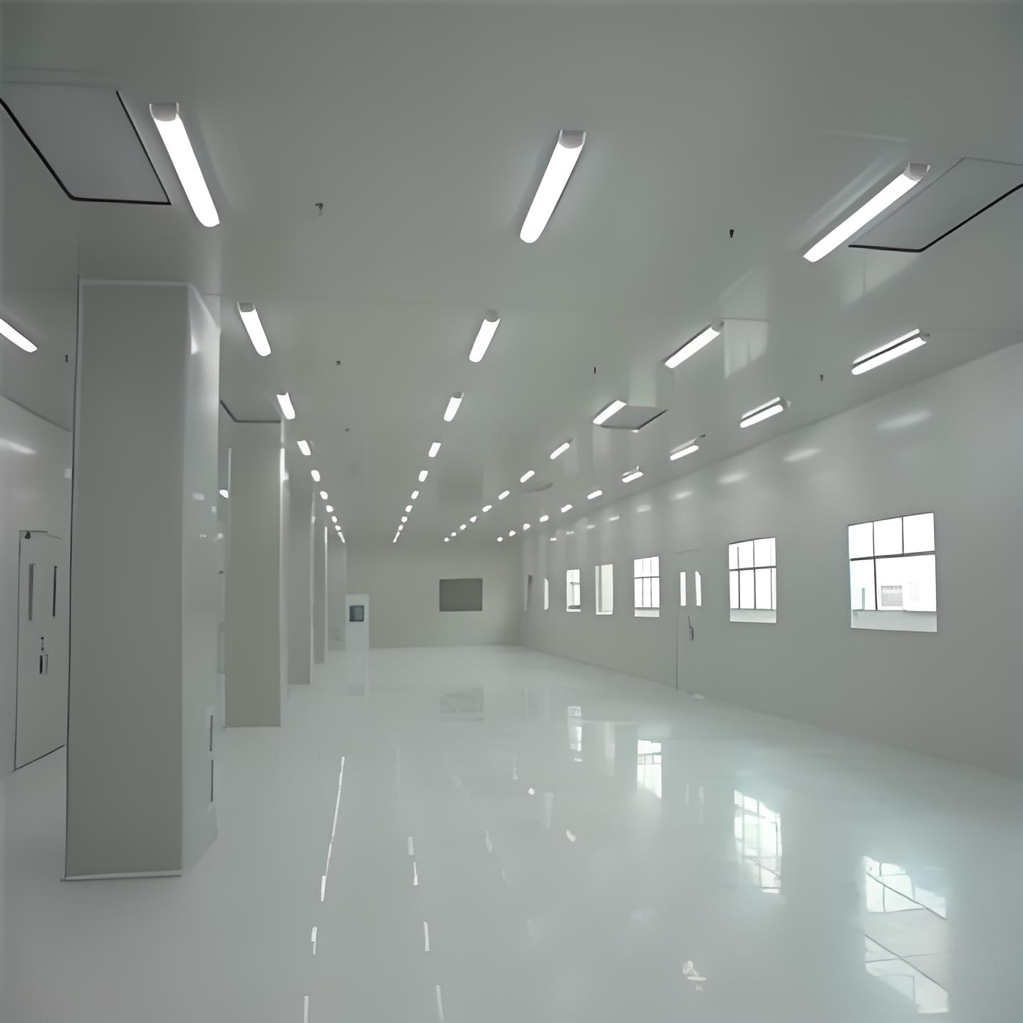

In high-density printed circuit board (PCB) assembly, surface mount technology (SMT), and semiconductor packaging, contamination is the primary driver of electrical failures, intermittent opens, and corrosion-induced breakdowns. A professionally executed Circuit board purification project establishes a controlled environment that removes particulate, ionic, and film-type residues from both the production atmosphere and the board surfaces themselves. Unlike general cleanrooms, PCB purification targets specific contaminants: solder flux residues, glass fiber dust, handling oils, and electrostatic-attached particles smaller than 1 µm. This article provides an engineering roadmap based on ISO 14644-1:2015, IPC-A-610, and J-STD-001, with practical solutions from TAI JIE ER, a specialist in turnkey cleanroom and contamination control systems.
Many electronics manufacturers mistake standard dust control for a proper Circuit board purification project. However, PCB production lines demand sub-ISO 7 environments with targeted removal of ionic residues (chlorides, bromides, weak organic acids) that cause dendritic growth. Below, we dissect eight essential technical pillars—from airborne particle management to board-level ionic cleanliness verification.
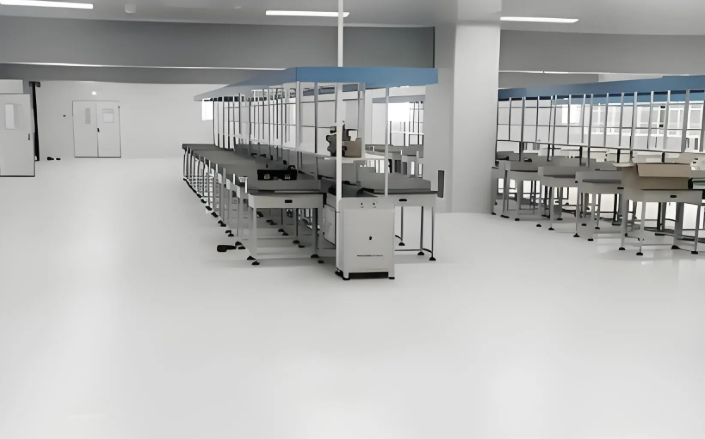
For SMT lines handling 01005 components or 0.3 mm pitch BGAs, the Circuit board purification project must maintain ISO 6 (Class 1,000) at rest and ISO 7 (Class 10,000) in operation, with critical zones like solder paste printing and underfill dispensing requiring ISO 5 laminar flow hoods. Key parameters:
HEPA/ULPA filtration: H14 grade for ISO 6 areas (≥99.995% at MPPS), U15 for ISO 5 zones. Filter face velocity: 0.45 m/s ±20%. Annual integrity testing per ISO 14644-3.
Air change rates: ISO 7 requires 30–60 ACH; ISO 6 requires 70–150 ACH. Recirculation air handlers with pre-filters (MERV 8) and final HEPA banks.
Positive pressure cascades: Minimum 10 Pa between clean corridor and SMT line, 15 Pa between printing zone and adjacent storage areas. Monitored by digital manometers with SCADA integration.
Real-time particle counters (0.3 µm and 0.5 µm channels) positioned near pick-and-place machines provide immediate feedback. For a recent wearable device manufacturer, TAI JIE ER designed a purification project that reduced airborne particle counts by 88% during solder paste printing, directly correlating to a 63% drop in tombstone defects.
Ionic contamination is a silent killer in PCB reliability. It originates from flux activators, handling sweat, and even ambient humidity carrying industrial pollutants. A thorough Circuit board purification project includes:
Chemical filtration (activated carbon + chemisorptive media): Removes volatile organic compounds (VOCs) and acidic gases (SO₂, NOₓ) from make-up air. Achieves ≤5 ppb of ionic precursors.
Board-level cleaning validation: Using ROSE (resistivity of solvent extract) testing per IPC-TM-650 2.3.25. Acceptable limit: ≤1.56 µg NaCl eq/cm² for high-reliability products. For no-clean fluxes, additional ion chromatography (IC) checks for chloride and weak organic acids.
In-line aqueous or semi-aqueous cleaning systems: For boards requiring high cleanliness, incorporate deionized water (18.2 MΩ·cm) rinsing with conductivity monitoring.
A case study: An automotive ECU supplier faced field failures due to dendrites between fine-pitch connectors. Their Circuit board purification project upgrade included a chemical filtration bank and weekly ROSE testing, reducing ionic contamination from 3.8 to 0.9 µg/cm², eliminating dendritic failures over 12 months.
ESD events attract airborne particles to charged board surfaces, defeating purification efforts. Moreover, ESD damage causes latent failures. An integrated purification project must include:
Static-dissipative flooring and work surfaces: Resistance 1×10⁶ to 1×10⁹ ohms. Grounding points every 30 m² with continuous monitoring.
Ionizing blowers (pulsed DC or steady-state): Positioned over PCB staging areas and before automated optical inspection (AOI). Balance voltage ≤ ±30 V.
Conductive HEPA filter frames: Standard anodized aluminum frames prevent static buildup. Cleanroom static control also includes anti-static smocks and wrist straps for operators.
Per ANSI/ESD S20.20, verification of ionizer offset voltage and discharge times (<2 seconds at 30 cm) should be performed quarterly.
Common hidden particle sources in PCB lines: conveyor belt wear, component tape debris, and solder ball splatter. A data-driven Circuit board purification project uses particle counters to map hotspots. Solutions:
Enclosing conveyors with acrylic shields and applying HEPA-filtered air sweeps at transfer points.
Using non-shedding conveyor belts (polyurethane or stainless steel mesh).
Installing vacuum extraction nozzles near stencil printers to capture excess solder paste particles.
Implementing sticky mats at all cleanroom entries and periodic tacky roller cleaning of equipment surfaces.
RH (relative humidity) between 40% and 55% is optimal: below 40% increases ESD risk; above 55% accelerates ionic migration and flux moisture absorption. Temperature: 22°C ±2°C. A purification project must include precision HVAC with ±2% RH control and dew point monitoring. Additionally, higher humidity increases particle adhesion to surfaces; however, laminar airflow velocities of 0.45 m/s keep particles suspended until HEPA capture.
Validation follows a structured lifecycle to ensure the Circuit board purification project meets IPC and customer specifications:
Installation Qualification (IQ): Verify FFU models, HEPA certificates, pressure differential transmitters, and ESD grounding continuity. Document materials of construction (non-outgassing polymers, stainless steel).
Operational Qualification (OQ): Smoke pattern visualization per ISO 14644-3: confirm unidirectional flow with no dead zones. Test alarm setpoints for particle count excursions. Measure air velocity uniformity (≤15% coefficient of variation).
Performance Qualification (PQ): Run three consecutive production shifts with actual PCBs. Sample for airborne particles every 10 minutes and collect surface particle samples (tape lift or vacuum). Conduct ROSE testing on test coupons. Acceptance criteria: ≥ISO 7 in dynamic mode; no visible residues under 10× magnification; ROSE ≤1.5 µg/cm².
Different electronics segments impose unique demands. Below are typical scenarios resolved by targeted purification projects.
High-frequency RF PCBs (5G, radar): Pain point – hydrophobic residues causing signal insertion loss. Solution – plasma cleaning (argon/oxygen) before conformal coating, integrated into the purification workflow.
Medical implantable electronics (pacemakers, neurostimulators): Pain point – biocompatibility requirements and zero whisker growth. Solution – use of Class ISO 5 cleanroom for final assembly, plus ultrasonic cleaning with deionized water and vacuum drying.
Automotive power modules (IGBT, SiC): Pain point – sulfur corrosion from ambient air (sulfur dioxide attacks silver-plated surfaces). Solution – installation of activated carbon + potassium permanganate chemical filters, and encapsulation of sensitive areas with conformal coating.
Semiconductor probe cards & burn-in boards: Pain point – sub-micron particle bridging between test probes. Solution – vertical laminar flow workstations with ULPA (U15) filters and sticky tacky rollers for frequent manual cleaning.
Through strategic Circuit board purification project design, TAI JIE ER solved a recurring yield issue for a satellite PCB manufacturer: outgassing contamination from low-quality gaskets. Replacing all polymeric seals with Viton® and adding a 48-hour bake-out step reduced particle fallout by 78%.
After commissioning, long-term success depends on:
Real-time particle counters connected to a data historian (e.g., OSIsoft PI). Alerts when counts exceed 50% of alarm limit.
Weekly surface cleanliness checks using portable particle counters (surface probe) and monthly ionic contamination testing via ROSE or ion chromatography.
Operator training on cleanroom behavior (no paper, no cardboard, proper gowning). Gowning qualification via particle shedding tests (Helmke drum or body box).
Scheduled requalification every 6 months for ISO 5 zones, annually for ISO 6-7 areas, per ISO 14644-2.
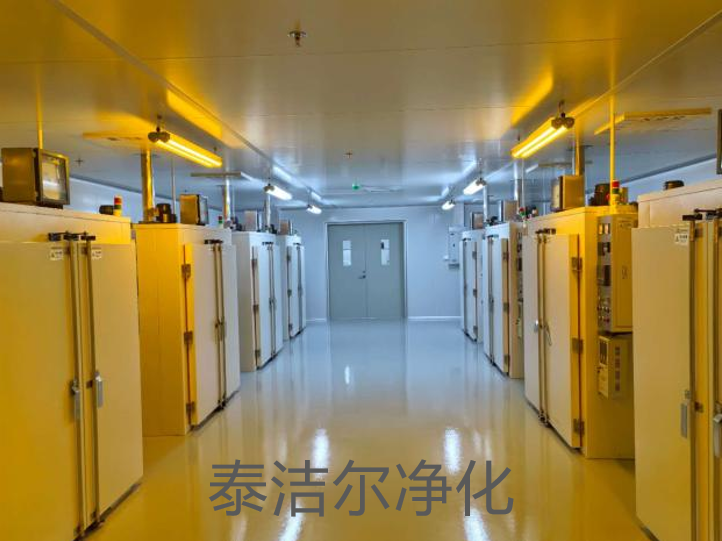
Executing a Circuit board purification project requires cross-domain knowledge: HVAC thermodynamics, ionic chemistry, ESD control, and PCB assembly processes. TAI JIE ER has delivered over 80 electronics cleanroom projects, including Class 10 (ISO 4) environments for wafer handling and ISO 6 SMT lines. Their approach includes:
Modular cleanroom panels with anti-static PVC surfaces, reducing construction time by 30% compared to conventional drywall.
In-house validation engineers who write IQ/OQ/PQ protocols meeting customer-specific IPC classifications.
Retrofit solutions for existing PCB lines – adding mini-environments and ionizers without stopping production.
A recent project for a defense contractor required an ISO 5 laminar flow zone for BGA rework stations. TAI JIE ER delivered a self-contained purification project with HEPA/ULPA fan-filter units, ESD flooring, and chemical filtration, achieving particle counts below 3,520 particles/m³ (≥0.5 µm) and ionic cleanliness of 0.7 µg/cm² – surpassing J-STD-001 requirements.
Q1: What is the minimum cleanroom classification for a circuit board
purification project serving SMT lines with 01005 components?
A1:
For reliable assembly of 01005 (0.4 mm × 0.2 mm) passives, the stencil printing
and pick-and-place zones require ISO 6 (Class 1,000) at rest and ISO 7 (Class
10,000) dynamic. The solder paste inspection area should have local ISO 5
laminar flow. For standard 0603 or larger components, ISO 8 may suffice, but
yield improves with ISO 7.
Q2: How often should we perform ionic contamination testing (ROSE)
within a purification project?
A2: For high-reliability products
(automotive, medical, aerospace), test every production shift or at least daily
using coupons. For consumer electronics, weekly testing is typical. Also perform
ROSE after any process change (new flux, new stencil cleaner, or after
maintenance of cleaning equipment).
Q3: Can we retrofit an existing SMT line with a purification project
without shutting down for weeks?
A3: Yes, using modular cleanroom
partitions and self-contained FFU arrays. Cleanroom retrofit engineering from TAI JIE
ER allows phased installation: first enclose the printer and dispenser, then the
placement machines, and finally the reflow oven zone. Typical retrofit takes 2–4
days per zone with production scheduled overnight or weekends.
Q4: What are the acceptance criteria for surface particle cleanliness
in a PCB purification project?
A4: Per IPC-A-610, no visible
particles under magnification of 10× for Class 2 and Class 3 assemblies. For
quantitative limits, using a tape lift method, ≤100 particles >50 µm per 100
cm² is common. For sub-50 µm particles, limits depend on component pitch; for
0.4 mm pitch BGAs, ≤10 particles >25 µm per component area is
recommended.
Q5: How does humidity control affect ionic
contamination?
A5: High relative humidity (>60%) accelerates
hygroscopic flux residue absorption of moisture, promoting ion migration and
electrochemical migration (ECM). Low humidity (<30%) increases electrostatic
attraction of particles and makes ionic residues more concentrated. Maintaining
40–55% RH is optimal; dehumidifiers and precision humidifiers are part of any
serious purification project.
Q6: What is the typical cost range for a turnkey circuit board
purification project for a 500 m² SMT facility?
A6: Costs vary by
classification, existing infrastructure, and region. A typical ISO 7 retrofit
with HEPA FFUs, chemical filtration, ESD flooring, and validation ranges from
$180,000 to $350,000. A new-build ISO 6 line with full HVAC and monitoring can
reach $500,000–$800,000. TAI JIE ER provides free feasibility
assessment and budget estimation based on your layout.
Contamination is not an inevitable cost of electronics manufacturing – it is a solvable engineering challenge. A well-specified Circuit board purification project reduces solder defects, prevents field failures from dendritic growth, and extends product lifespan. From airborne HEPA filtration to board-level ionic cleanliness validation, each pillar contributes to measurable return on investment through higher first-pass yields and lower warranty claims.
Partner with a proven cleanroom specialist to design, build, and validate your purification infrastructure. TAI JIE ER offers turnkey services including cleanroom construction, chemical filtration integration, ESD protection, and full documentation for regulatory compliance (ISO, IPC, J-STD). Their engineering team provides on-site support from concept to operational handover.
Ready to discuss your Circuit Board Purification
Project?
Request a no-obligation technical consultation and
budgetary quote. Provide your production volume, component pitch, current defect
rates, and floor plan. Contact TAI JIE ER via the official website or
email directly to sales@taijieer.com. Mention “PCB Purification Project” for
priority engineering review. We will respond within 24 hours with a customized
proposal including cleanroom class recommendation, equipment list, validation
timeline, and cost breakdown.