In high-density interconnect (HDI) and multilayer printed circuit board (PCB) fabrication, even submicron contaminants can lead to dielectric breakdown, corrosion, or assembly failures. A structured Circuit board purification project goes beyond conventional cleaning—it integrates controlled environment strategies, validated process chemistries, and real-time verification. This article provides an in-depth look at contamination sources, process architecture, and performance verification methods tailored for B2B clean engineering environments. Drawing on established practices from TAI JIE ER, we examine how systematic purification projects directly affect product reliability and manufacturing yield.
Standard washing or manual wipe-downs are insufficient for modern electronics. Residues from soldering fluxes, plating baths, and handling can remain trapped under components or within micro-vias. A dedicated Circuit board purification project is mandatory for industries such as aerospace, medical devices, automotive radar, and 5G infrastructure, where field failures have severe consequences. The core drivers include:
Ionic residues (chlorides, bromides, acids): Promote electrochemical migration and dendrite growth.
Particulate contamination (dust, fibers, metal fragments): Cause shorts or interfere with conformal coating adhesion.
Organic films (flux residues, oils, handling marks): Affect soldering wetting and surface insulation resistance (SIR).
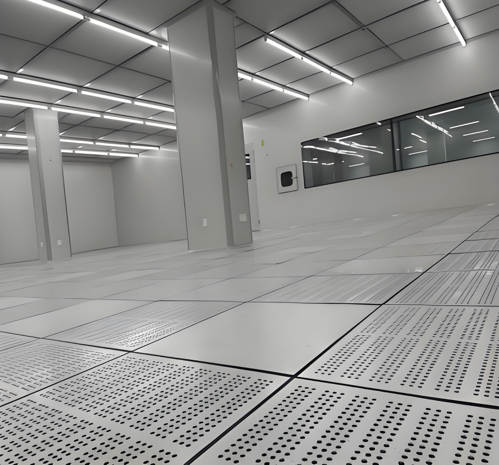
Without a comprehensive purification methodology, even advanced substrate materials cannot achieve their rated performance. Leading contract manufacturers therefore adopt standardized purification protocols that align with IPC-5704 and ISO 14644-1 cleanroom classifications.
Before designing any purification workflow, engineers must identify specific contamination vectors. Common sources include:
Wet processing stages: Developing, etching, and stripping baths leave ionic residues if rinsing is insufficient.
Reflow and wave soldering: Rosin-based and no-clean flux residues become trapped under BGAs or QFNs.
Mechanical handling: Fingerprints, glove particles, and conveyor belt abrasion generate organic and particulate debris.
Ambient air quality: Unfiltered facility air introduces fibers, dust, and volatile organic compounds (VOCs).
A properly scoped Circuit board purification project begins with contamination mapping—using ion chromatography, particle counters, and Fourier-transform infrared (FTIR) spectroscopy to classify residues. This diagnostic step ensures that cleaning chemistry and mechanical action are precisely targeted.
Effective purification relies on three interdependent systems: media (chemistry & water), mechanical energy (spray, immersion, or ultrasonics), and environmental control (cleanroom airflow). Below are the essential building blocks:
Single-pass tap water introduces minerals and bacteria. Industry-grade purification uses two-stage reverse osmosis (RO) followed by electrodeionization (EDI), achieving resistivity ≥18 MΩ·cm. Cascade rinsing with conductivity monitoring ensures ionic removal down to parts-per-billion levels.
Depending on residue polarity, engineers select from saponifiers, terpene-based solvents, or semi-aqueous formulations. Critical parameters: pH, temperature (50–70°C), and dwell time. For no-clean flux residues, a controlled circuit board purification project often employs micro-emulsion chemistry that lifts polymer networks without attacking solder mask.
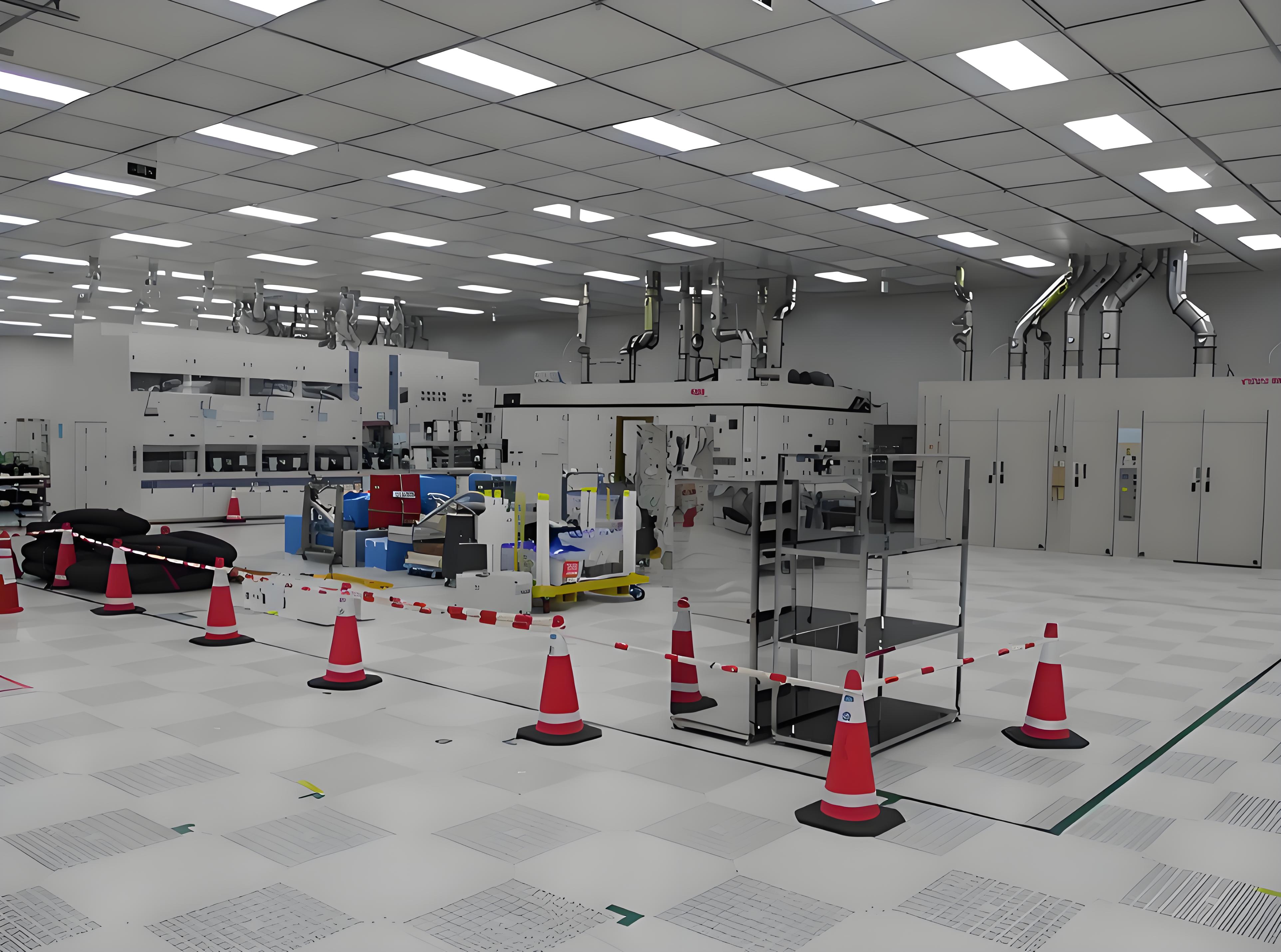
Purification is not just about wet cleaning; dry processing steps must occur in ISO Class 5 or better mini-environments. Fan filter units (FFUs) with ULPA filters (99.9995% efficiency at 0.12 µm) maintain particle counts below 3520 particles/m³ for ≥0.1 µm.
Humidity and stagnant droplets re-deposit dissolved ions. Multi-stage hot-air drying with anti-static nozzles, followed by vacuum-assisted drying ovens, prevents water spots and oxidation. Integrated conductivity probes verify final rinse purity before boards exit the purification tunnel.
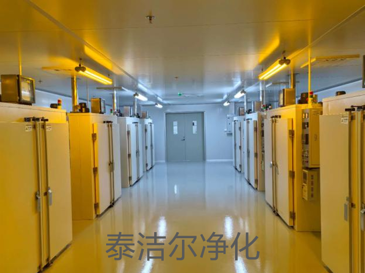
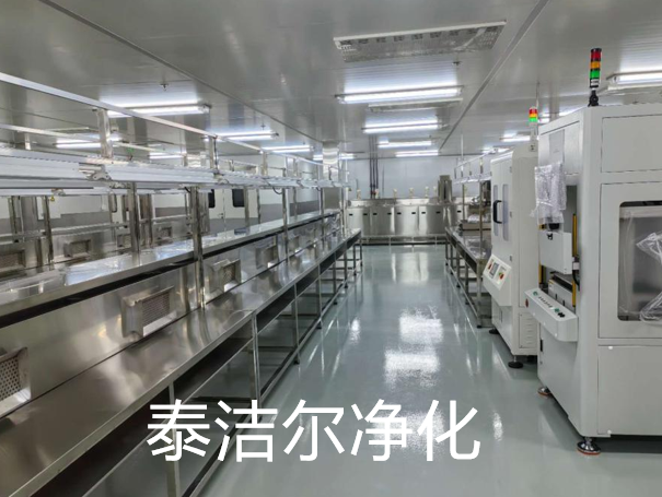
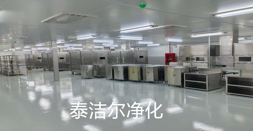
The following sequence represents a validated workflow commonly deployed by TAI JIE ER for mission-critical PCB assemblies. Each step includes in-line verification to enable real-time adjustments.
Pre-wash inspection & contamination mapping: Automated optical inspection (AOI) combined with ionograph testing establishes baseline cleanliness (ROSE, SIR).
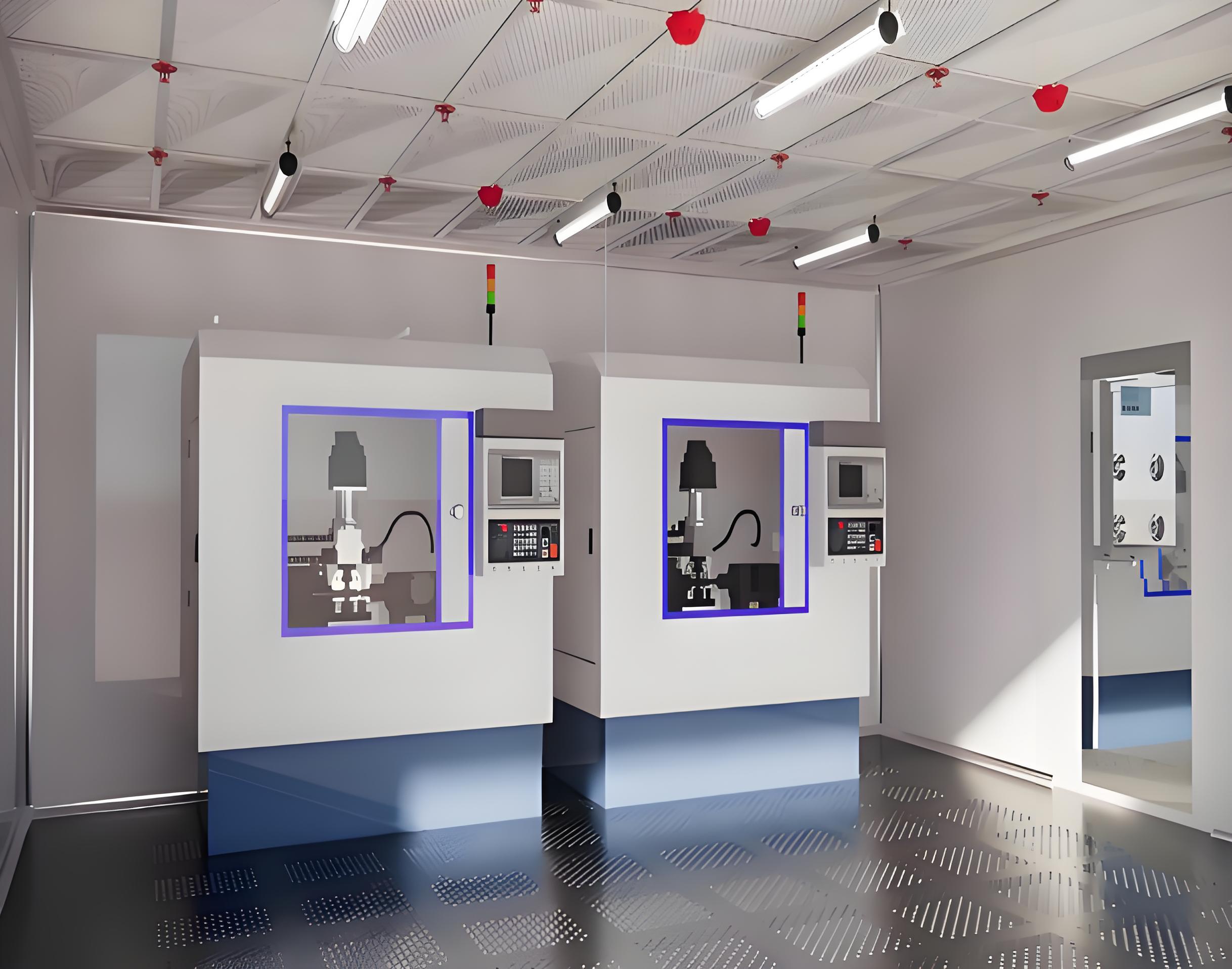
Chemical application stage: Spray-under-immersion or ultrasonic cavitation with pH-stabilized cleaning agent. Mechanical agitation dislodges encapsulated residues from via holes.
Intermediate cascade rinses: Three to five counter-flow deionized water baths, each with conductivity sensors. Water quality improves progressively, avoiding cross-contamination.
Final high-pressure DI rinse: Oscillating nozzles at 5–8 bar pressure remove remaining particles < 5 µm. Deionized water at 60°C improves ionic solubility.
Hot-air knife drying & infrared preheat: Removal of surface moisture before vacuum thermal cycle (100–130°C, 30 min) to eliminate entrapped humidity in laminates.
Post-purification verification: SIR testing under bias-humidity (85°C/85% RH, 168 hours), ionic cleanliness by ion chromatography (per IPC-TM-650).
Each Circuit board purification project demands tunable parameters based on board geometry and component sensitivity. For example, MEMS devices require reduced ultrasonic power to prevent wire-bond damage, while rigid-flex boards need modified drying profiles to avoid layer delamination.
Different end-markets impose unique cleanliness thresholds, driving customized project configurations:
High-Frequency PCBs (RF/microwave): Low-loss materials (e.g., PTFE) are sensitive to chemical absorption. Projects use specially formulated fluorinated solvents and plasma-based dry purification.
Automotive power electronics: Thick copper substrates and thermal vias require aggressive saponifier pre-soak to remove oxidized residues after soldering.
Medical implantable devices: Zero ionic residues mandated; purification project includes multiple extractive sampling and endotoxin control.
Aerospace & defense: Conformal coating adhesion demands both organic and particulate removal to level N+3 per MIL-STD-883.
Forward-thinking facilities integrate statistical process control (SPC) and predictive maintenance into their purification lines. Key enablers include:
Inline total organic carbon (TOC) sensors, resistivity meters, and particle counters in the recirculating DI loop provide early warning of filter breakthrough or chemistry depletion. Alerts trigger automatic bleed-and-feed actions without stopping production.
Each carrier or panel receives an RFID tag storing process parameters (wash pressure, bath temperature, conductivity). This data feeds into MES software for SPC charts—enabling root cause analysis when field returns occur.
For components where wet cleaning is impractical (e.g., sensor arrays or pre-bonded stacks), low-pressure argon/oxygen plasma removes organic films atomically. CO₂ snow jets eliminate particles down to 0.2 µm without residue. Many purification projects combine wet and dry stages for optimal results.
Executing a robust Circuit board purification project requires interdisciplinary knowledge—fluid mechanics, surface chemistry, and contamination control. TAI JIE ER provides engineered solutions based on decades of clean process integration. Their approach starts with a contamination audit and ends with validated, document-ready verification protocols. The company’s modular purification platforms allow electronics manufacturers to scale from batch to inline processing without re-engineering core workflows. By using closed-loop DI systems and low-VOC chemistries, TAI JIE ER helps clients meet both IPC Class 3 standards and sustainability goals.
Beyond equipment specification, the firm offers remote process monitoring dashboards and annual recertification services. This ensures that your purification project continues performing as line speeds or product mixes evolve. For enterprises seeking to reduce field failure rates and warranty claims, partnering with an expert integrator is a determinant of success.
The gap between standard cleaning and a professionally engineered Circuit board purification project directly translates to product lifecycle performance. With rising electrical demands (higher voltage, finer pitch) and harsh-environment applications, controlling ionic, organic, and particulate contaminants is no longer optional. A well-designed project reduces infant mortality failures, enhances insulation resistance, and ensures conformity to industry reliability standards. When selecting a purification partner, prioritize those with demonstrable process engineering capabilities—like TAI JIE ER—who can adapt parameters to your specific substrates, assembly types, and cleanliness metrics.
Q1: What differentiates a
professional circuit board purification project from routine board
washing?
A1: Routine washing typically uses generic detergents and
single-rinse cycles without monitoring. A professional purification project
includes contamination pre-mapping, deionized cascade rinses with resistivity
feedback, residue-specific chemistries, and post-clean verification (e.g., SIR,
ionic contamination testing). It also mandates cleanroom handling after drying
to prevent recontamination.
Q2: How frequently should purification
parameters be revalidated?
A2: At minimum, quarterly revalidation of
chemical concentration, DI water resistivity, nozzle pressure uniformity, and
drying oven temperature profile. Any change in board design, flux type, or
soldering profile triggers a full revalidation. In high-reliability sectors
(medical/aerospace), monthly verification with coupon testing is common.
Q3: Which contaminants are most challenging to remove from high-density
circuit boards?
A3: Three categories cause most failures: (1)
encapsulated no-clean flux residues beneath BGA standoffs—require high-pressure
micro-spray or vapor degreasing; (2) inorganic salts (e.g., nickel chloride from
plating) that adsorb into hole walls—needs extended ionic exchange baths; (3)
silicone-based oils from handling—demand fluorinated or modified alcohol
chemistries.
Q4: Can a purification project improve performance for
legacy or reworked PCBs?
A4: Yes, properly executed purification
removes oxidized residues and ionic contamination that accumulate during rework
or extended storage. It can restore surface insulation resistance and reduce
leakage current. However, caution is required with aged laminates to avoid
delamination; a controlled low-temperature process is recommended.
Q5:
How does the purification project affect subsequent assembly processes like
conformal coating or underfill?
A5: A correctly performed
purification leaves a chemically clean, high-surface-energy condition, which
improves wetting and adhesion of conformal coatings, underfills, and staking
compounds. Conversely, residual non-polar solvents or surfactants can cause
dewetting. Therefore, final rinse and bake parameters are selected to maximize
surface compatibility.
Q6: What documentation should a B2B buyer request
for a purification project validation?
A6: Buyers should request a
validation protocol including: ion chromatograph reports for specific
anions/cations, particle count data (per ISO 14644), SIR testing graphs
(85°C/85% RH for 168h), and batch records showing process parameters (pressure,
temperature, conductivity trends). Also require a statistical process control
(SPC) capability study (Cpk ≥ 1.33).
Every circuit board purification project must be tailored to your materials, flux types, and reliability targets. Whether you are upgrading an existing cleaning line or designing a new cleanroom workflow, our engineering team provides contamination audits, process design, and turnkey verification. Share your specifications to receive a customized proposal that aligns with IPC, J-STD, or your internal quality benchmarks.
Send your inquiry now – provide board dimensions, annual volume, and required cleanliness class. Our specialists will respond with a preliminary process flow and performance guarantees.
Contact TAI JIE ER directly through the website or request a call to discuss your Circuit board purification project roadmap.