In today's fast-paced electronics industry, the demand for reliable and high-performance printed circuit boards (PCBs) is higher than ever. A well-executed Circuit board purification project is essential to minimize contaminants, reduce defects, and enhance product longevity. This article delves into the critical aspects of creating controlled environments for PCB fabrication, highlighting how proper cleanroom setups, ESD controls, and filtration systems can transform manufacturing outcomes. Whether you're an engineer, project manager, or industry stakeholder, understanding these elements can help you achieve superior results in your PCB cleanroom facility project. We'll explore practical steps, from designing a controlled environment for PCB fabrication to selecting experienced cleanroom contractors for electronics industry, ensuring your facility meets stringent quality standards. By the end, you'll have a clear roadmap for implementing a successful purification initiative that aligns with modern electronics demands.
A Circuit board purification project focuses on eliminating particulate, chemical, and electrostatic discharge (ESD) threats during PCB manufacturing. This involves integrating advanced filtration, climate control, and specialized cleanroom designs to maintain an ultra-clean environment. Such projects are vital in industries like aerospace, medical devices, and consumer electronics, where even minor contaminants can lead to costly failures. For instance, dust particles or chemical residues can cause short circuits or corrosion, compromising board integrity. By prioritizing purification, companies can improve yield rates, reduce rework, and comply with international standards like ISO 14644 for cleanrooms. A typical project includes phases like assessment, design, implementation, and validation, often requiring collaboration with experts in PCB facility with particulate and chemical filtration. This holistic approach ensures that every aspect of the manufacturing process is optimized for cleanliness and efficiency, making the Circuit board purification project a cornerstone of quality assurance in electronics production.
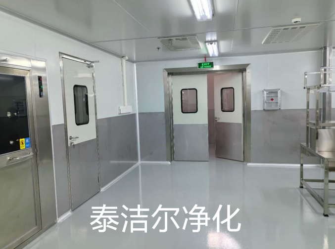
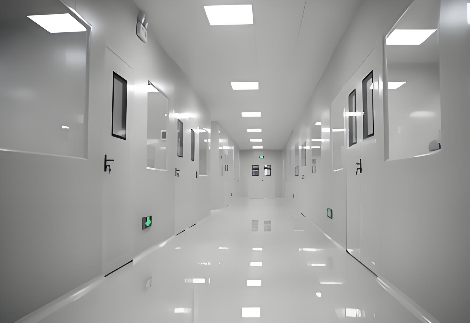
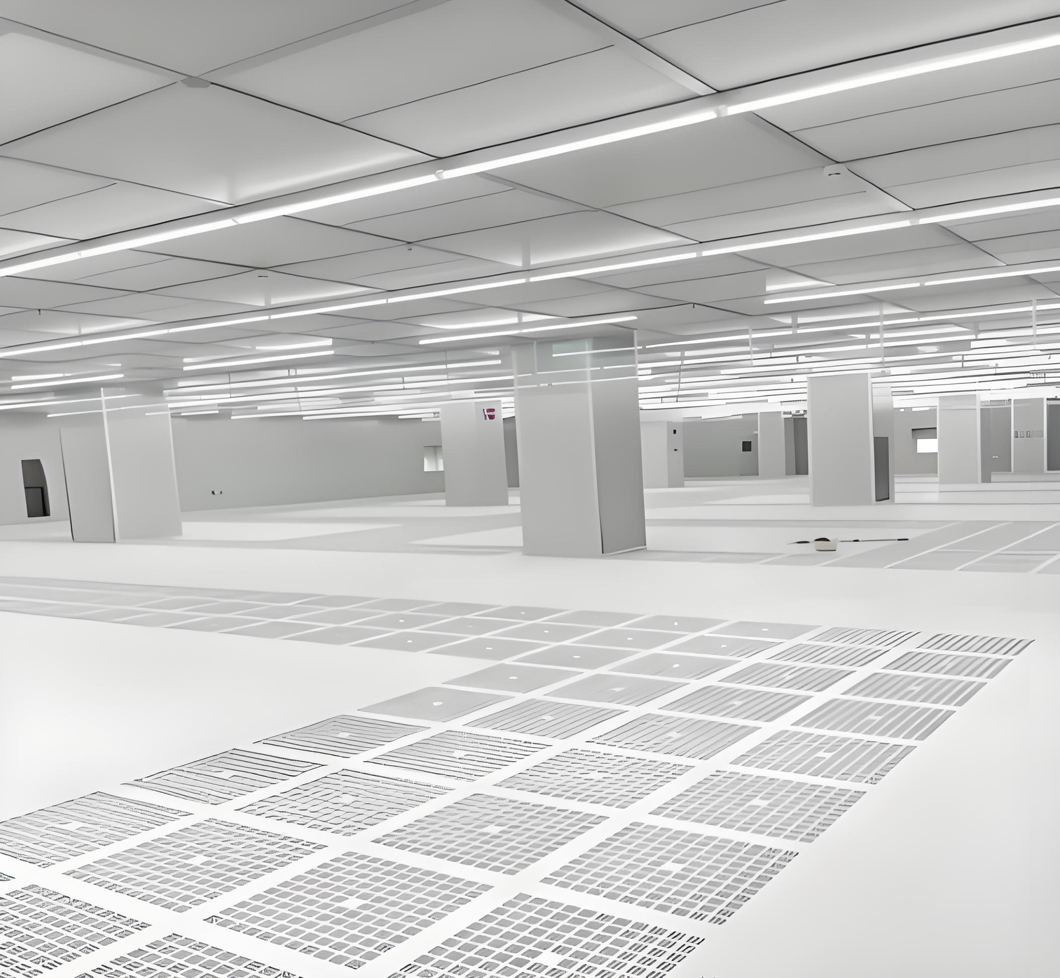
Creating a controlled environment for PCB fabrication is the first step in any Circuit board purification project. This environment regulates temperature, humidity, and air quality to prevent contamination and ensure consistent PCB performance. Key components include HVAC systems with HEPA filters, which remove airborne particles, and precise climate control to avoid moisture-related issues like delamination. For example, in a PCB cleanroom facility project, maintaining a humidity level of 40-60% can prevent static buildup and material degradation. Additionally, the layout should separate high-contamination areas, such as soldering stations, from clean zones to minimize cross-contamination. Implementing a controlled environment for PCB fabrication also involves using non-shedding materials for walls and floors, along with positive air pressure to keep contaminants out. This setup not only supports the goals of a Circuit board purification project but also enhances worker safety and operational efficiency. By investing in such environments, manufacturers can achieve higher precision in multilayer PCB production and extend the lifespan of their equipment.
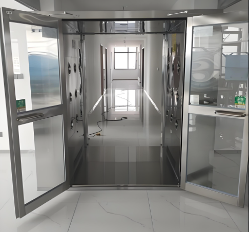
A cleanroom with ESD control for electronics is crucial in a Circuit board purification project to protect sensitive components from electrostatic discharge, which can damage microchips and circuits. ESD events, often caused by human contact or ungrounded equipment, can lead to latent defects that are hard to detect. To mitigate this, a cleanroom with ESD control for electronics incorporates grounded workstations, anti-static flooring, and ionizers to neutralize charges. Personnel must wear ESD-safe attire, including wrist straps and smocks, while tools and containers should be made of dissipative materials. In the context of a PCB cleanroom facility project, integrating ESD controls with particulate management ensures comprehensive protection. For instance, combining HEPA filtration with ESD safeguards in a single cleanroom with ESD control for electronics can reduce defect rates by over 50%. This synergy is a hallmark of an effective Circuit board purification project, as it addresses both visible and invisible threats to PCB integrity. Regular audits and training further reinforce these measures, making the facility resilient to ESD-related failures.
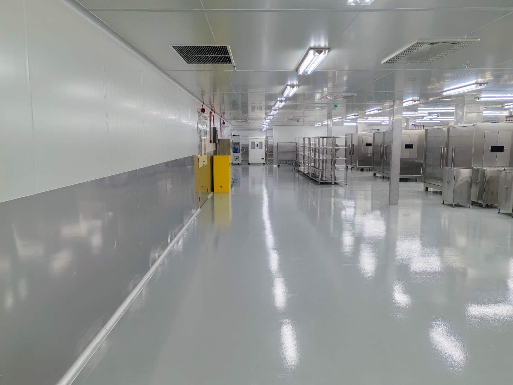
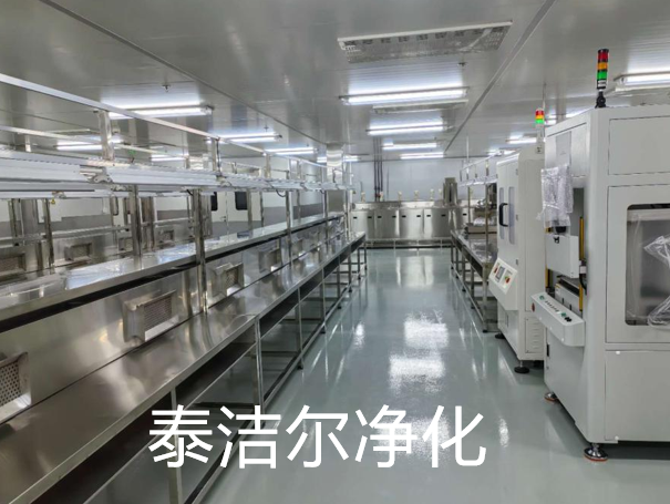
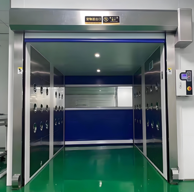
A PCB facility with particulate and chemical filtration is engineered to remove both solid and gaseous contaminants, playing a pivotal role in a Circuit board purification project. Particulate filtration, using HEPA or ULPA filters, captures dust, fibers, and microbes that could impair circuit connections. Meanwhile, chemical filtration systems, such as activated carbon scrubbers, absorb volatile organic compounds (VOCs) and acids that might cause corrosion. In a typical PCB cleanroom facility project, these systems are integrated into the ventilation to maintain air quality below Class 1000 cleanroom standards. For example, in a PCB facility with particulate and chemical filtration, real-time monitoring sensors can alert staff to contamination spikes, allowing for immediate corrective actions. This proactive approach aligns with the objectives of a Circuit board purification project by ensuring that boards are produced in a pristine environment. Moreover, such facilities often feature automated material handling to minimize human-induced contaminants, further supporting the purification goals. By optimizing filtration, manufacturers can achieve higher reliability in high-frequency and miniaturized PCBs, meeting the demands of advanced applications like 5G and IoT.
A successful PCB cleanroom facility project requires meticulous planning, from conceptual design to commissioning, as part of a broader Circuit board purification project. This involves defining cleanroom classifications based on product requirements—for instance, Class 100 for critical assemblies or Class 1000 for less sensitive areas. Key steps include conducting a risk assessment to identify contamination sources, budgeting for infrastructure like laminar flow hoods, and scheduling phased implementations to avoid production disruptions. Collaboration with stakeholders, including cleanroom contractors for electronics industry, is essential to align the project with regulatory standards and operational needs. During execution, aspects like validation testing (e.g., particle counts and airflow visualization) ensure the facility performs as intended. A well-managed PCB cleanroom facility project not only supports the Circuit board purification project but also offers scalability for future expansions. For example, incorporating modular cleanroom designs allows easy upgrades to accommodate new technologies. By following best practices in project management, companies can minimize downtime and maximize return on investment, making the purification initiative a long-term asset.
Choosing experienced cleanroom contractors for electronics industry is a critical decision in any Circuit board purification project. These specialists provide expertise in design, construction, and certification, ensuring that the cleanroom meets specific electronics manufacturing needs. When evaluating cleanroom contractors for electronics industry, look for a proven track record in projects similar to your PCB cleanroom facility project, including experience with ESD controls and filtration systems. Key criteria include certifications like ISO 9001, the ability to customize solutions, and post-installation support for maintenance. For instance, a contractor might recommend energy-efficient systems for a PCB facility with particulate and chemical filtration to reduce operational costs. Involving cleanroom contractors for electronics industry early in the planning phase can help avoid common pitfalls, such as inadequate space allocation or compliance issues. This partnership is integral to the success of a Circuit board purification project, as it translates technical requirements into a functional environment. By selecting reputable contractors, manufacturers can ensure their facility adheres to industry benchmarks, ultimately enhancing product quality and competitiveness.
As electronics evolve toward smaller, more complex designs, the importance of a Circuit board purification project will only grow. Emerging trends include the integration of IoT sensors for real-time environmental monitoring and the use of sustainable materials in cleanroom construction. Advances in PCB facility with particulate and chemical filtration may incorporate AI-driven predictive maintenance to optimize filter life and energy use. Moreover, global standards are becoming stricter, necessitating continuous improvement in controlled environment for PCB fabrication. Companies that prioritize these aspects in their PCB cleanroom facility project will lead in innovation, reducing waste and boosting reliability. Ultimately, a forward-thinking Circuit board purification project not only addresses current challenges but also prepares facilities for future technologies like flexible electronics and quantum computing. By staying updated with industry shifts and collaborating with skilled cleanroom contractors for electronics industry, businesses can maintain a competitive edge while upholding the highest cleanliness standards.
In summary, a well-planned Circuit board purification project is indispensable for achieving excellence in PCB manufacturing. By focusing on elements like a controlled environment for PCB fabrication, a cleanroom with ESD control for electronics, and a PCB facility with particulate and chemical filtration, companies can significantly reduce defects and enhance product performance. Engaging with proficient cleanroom contractors for electronics industry ensures that every phase of the PCB cleanroom facility project is executed to perfection. As the electronics landscape advances, investing in such purification initiatives will remain a key differentiator for quality and innovation. Start your journey today by assessing your facility's needs and building a robust strategy for purification.
Q1: What is the primary goal of a circuit board purification project?
A1: The main goal of a circuit board purification project is to create a manufacturing environment that minimizes contaminants like dust, chemicals, and electrostatic discharge, thereby reducing PCB defects, improving reliability, and ensuring compliance with industry standards.
Q2: How does a controlled environment for PCB fabrication contribute to product quality?
A2: A controlled environment for PCB fabrication maintains stable temperature, humidity, and air purity, which prevents issues such as moisture absorption, oxidation, and particulate contamination. This leads to higher yield rates, longer board lifespan, and consistent performance in end-products.
Q3: Why is ESD control important in a cleanroom for electronics?
A3: ESD control in a cleanroom with ESD control for electronics is vital because electrostatic discharge can damage sensitive electronic components, causing latent failures or immediate malfunctions. Implementing ESD safeguards, like grounding and ionizers, protects PCBs during handling and assembly, ensuring overall project success.
Q4: What are the key features of a PCB facility with particulate and chemical filtration?
A4: A PCB facility with particulate and chemical filtration typically includes HEPA/ULPA filters for removing airborne particles and chemical scrubbers for eliminating VOCs and corrosive gases. These features help maintain a clean environment, crucial for a circuit board purification project, by preventing contamination that could impair circuit integrity.
Q5: How do I choose the right cleanroom contractors for an electronics industry project?
A5: Select cleanroom contractors for electronics industry based on their experience with similar projects, relevant certifications, ability to customize designs, and post-installation support. It's important to review their portfolio and ensure they understand the specific needs of a PCB cleanroom facility project to achieve optimal results.
Q6: What common challenges arise during a PCB cleanroom facility project, and how can they be addressed?
A6: Common challenges in a PCB cleanroom facility project include budget overruns, compliance issues, and integration with existing systems. These can be addressed by thorough planning, involving experts early, and choosing flexible designs. Working with experienced cleanroom contractors for electronics industry can help mitigate risks through proactive problem-solving.