Electronic Purification Engineering is the critical, often unseen, discipline that makes modern technology possible. It encompasses the entire ecosystem of designing, constructing, and maintaining ultra-low contamination environments essential for manufacturing semiconductors, microchips, photovoltaics, and other high-precision electronics. Without advanced electronic purification engineering, the relentless march of Moore's Law would grind to a halt. This comprehensive guide delves into the core components of this field, from the foundational principles of Electronics Cleanroom Engineering to the intricate management of Semiconductor Fab Facility Construction, highlighting common challenges and the integrated solutions that ensure success.
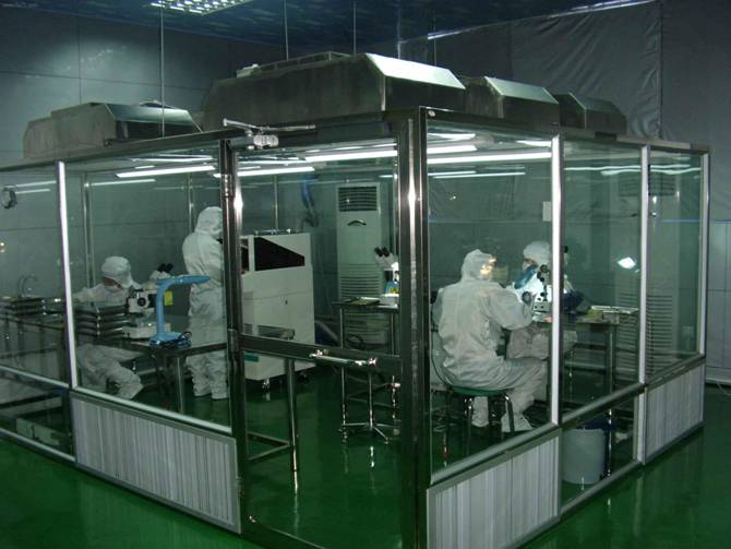
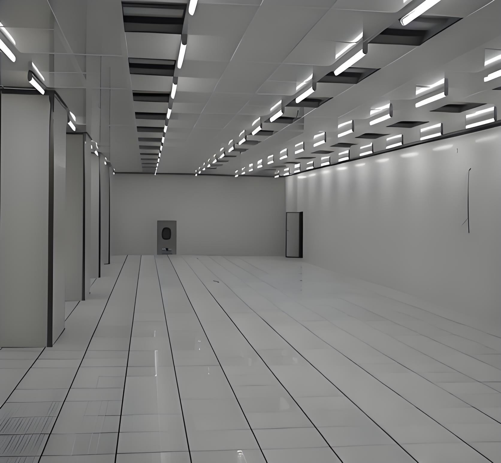
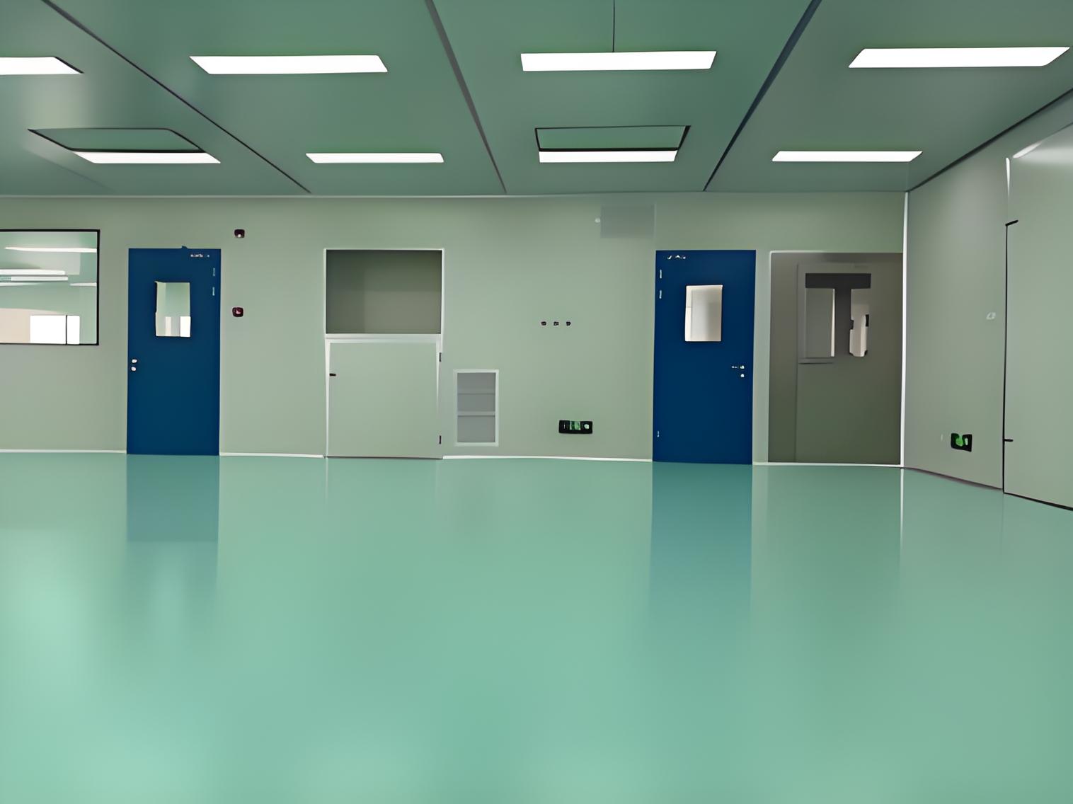
At the heart of electronic purification engineering lies Electronics Cleanroom Engineering. This is not merely about creating a "clean room"; it is about designing a hyper-specialized, controlled environment where parameters like airborne particulate count, temperature, humidity, pressurization, and static electricity are meticulously regulated.
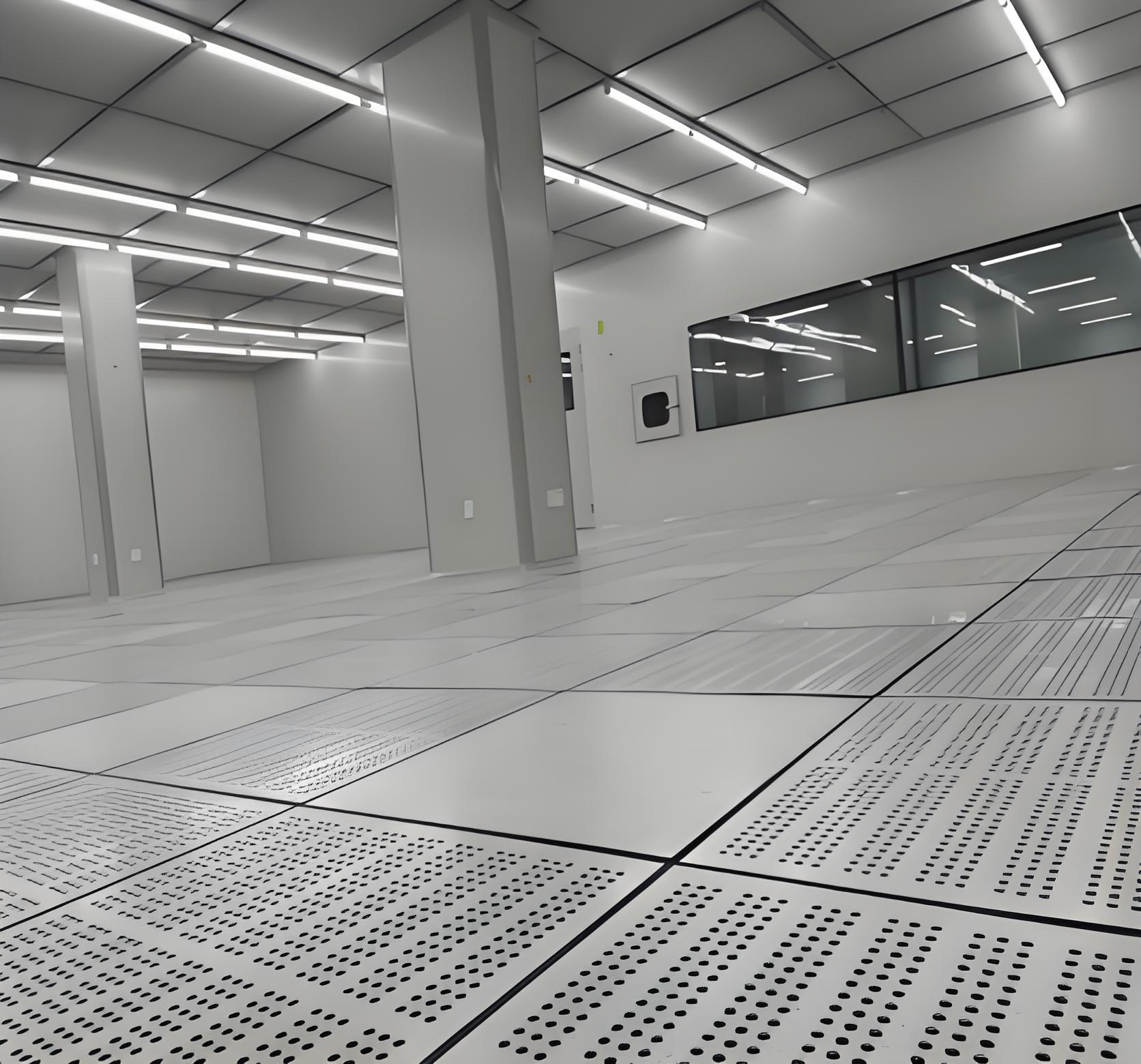
Cleanrooms are classified by the number and size of particles permitted per volume of air. For instance, an ISO Class 5 cleanroom (equivalent to Class 100) allows no more than 3,520 particles of 0.5 microns per cubic meter—a stark contrast to the millions of particles found in ordinary urban air. Achieving this requires a complex orchestration of:
High-Efficiency Particulate Air (HEPA) and Ultra-Low Penetration Air (ULPA) Filters: These filters remove up to 99.9995% of particles from the air supply.
Laminar and Turbulent Airflow Systems: Directional, smooth (laminar) airflow sweeps contaminants away from the product, while non-directional (turbulent) airflow dilutes and removes contamination through repeated air changes.
Advanced Materials: Walls, ceilings, and floors are constructed using non-shedding, smooth, and static-dissipative materials to minimize particle generation.
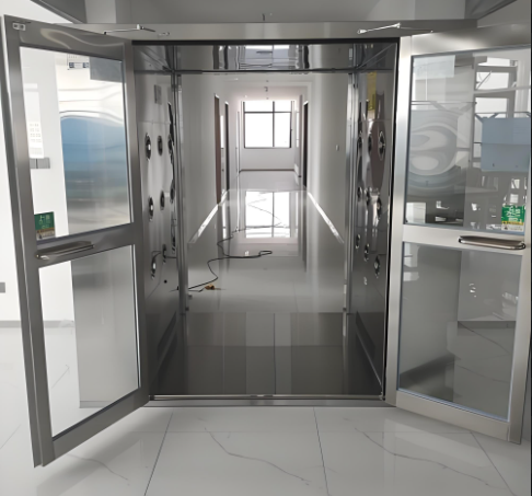
Strict Gowning Protocols: Personnel must wear bunny suits, gloves, masks, and booties to contain human-borne contaminants.
Common Problem: A frequent issue in Electronics Cleanroom Engineering is inadequate airflow planning. Poorly designed airflow can create "dead zones" where particles accumulate or eddies that carry contaminants directly to the product wafer, leading to catastrophic yield loss.
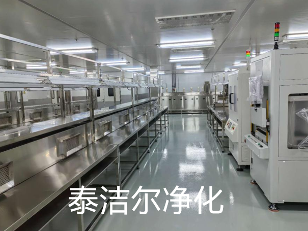
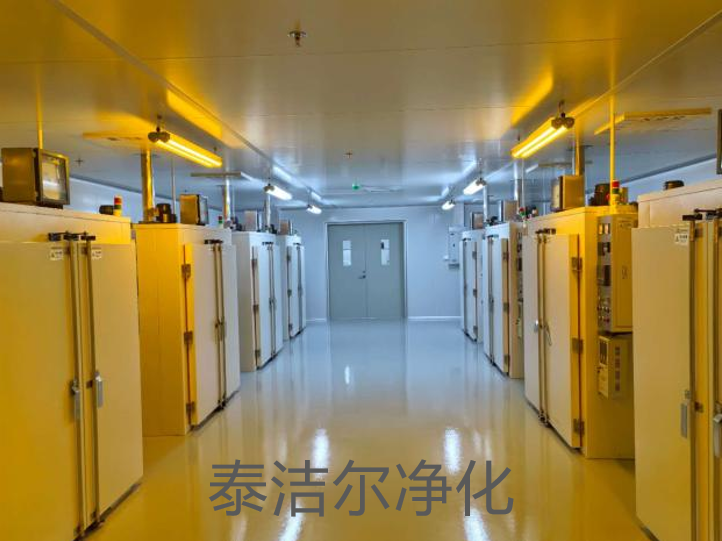
Semiconductor Fab Facility Construction is arguably one of the most complex and capital-intensive endeavors in the industrial world. A new fab can cost billions of dollars and take several years to complete. This goes far beyond the cleanroom itself; it involves building a "city within a city" that includes:
Ultra-Pure Water (UPW) Plants: Water used in etching and cleaning must be purified to an extraordinary degree, often exceeding 18 megohm-cm resistivity.
Specialty Gas Systems: Highly toxic, corrosive, and pyrophoric gases (like arsine and silane) require double-contained piping and ultra-leak-proof delivery systems.
Vibration-Sensitive Foundations: The entire fab must be isolated from external vibrations to protect sensitive lithography scanners.
Redundant Utility Systems: Continuous power, process cooling water, and bulk gas supplies are backed up by extensive redundancy to prevent billions of dollars in losses from an unplanned shutdown.
Common Problem: The sheer scale and interdependency of systems lead to significant coordination challenges. A delay in the delivery of one specialized system, like the UPW plant, can create a critical path delay for the entire Semiconductor Fab Facility Construction project, inflating budgets and pushing back production timelines.
To mitigate the risks and complexities inherent in such projects, many companies opt for Turnkey Cleanroom Solutions. This approach involves contracting a single provider—or a primary contractor with deeply integrated partners—to handle the entire project from concept to certification. This "single responsibility" model covers:
Initial Design and Consultation
Procurement of All Materials and Equipment
Construction and Installation
Integration of Mechanical and Electrical Systems
Final Certification and Handover
The major advantage of Turnkey Cleanroom Solutions is the seamless accountability. Instead of managing dozens of subcontractors and dealing with finger-pointing when issues arise, the client has one point of contact responsible for delivering a fully functional facility that meets all specifications.
Common Problem: Without a true turnkey model, the interface between different subcontractors (e.g., between the HVAC installer and the controls integrator) becomes a major point of failure. Communication gaps and unclear scopes of work can result in systems that do not communicate properly, leading to performance failures.
A cleanroom is not operational simply because construction is finished. It must undergo rigorous Cleanroom Certification and Testing to verify that it performs exactly as designed according to international standards like ISO 14644-1. This critical phase of electronic purification engineering involves a battery of tests:
Airborne Particle Count: Measuring particulate levels to verify the ISO class in various states (as-built, at-rest, operational).
Airflow Velocity and Volume: Ensuring HEPA/ULPA filters are delivering the required cubic feet per minute (CFM) of air.
Room Pressurization: Testing that the cascade of pressure (from cleanest to least clean areas) is maintained to prevent infiltration of dirty air.
HEPA/ULPA Filter Integrity: Using a photometer or particle counter with a polydisperse aerosol challenge to detect any filter leaks.
Temperature and Humidity Uniformity: Mapping the entire space to ensure tight control of these critical parameters.
Common Problem: A common and serious issue is discovering that the cleanroom fails to meet its ISO classification during operational testing. This is often traced back to construction debris left in ductwork, compromised filter seals during installation, or unsealed penetrations in the cleanroom envelope for utilities and conduits.
In the nanoscale world of semiconductor manufacturing, even the slightest vibration can be disastrous. Vibration Analysis and Mitigation is a highly specialized niche within electronic purification engineering that focuses on identifying and isolating equipment from vibrational energy.
Lithography tools, which project circuit patterns onto silicon wafers with features smaller than a virus, are exceptionally sensitive. Vibrations from nearby roads, building HVAC systems, or even footsteps can cause blurring and misalignment, rendering chips defective. The process involves:
Site Vibration Survey: Measuring existing ambient vibration levels at a greenfield site before construction begins.
Predictive Modeling: Using data to model how the proposed building structure will respond to vibrational inputs.
Designing Isolation Systems: Implementing massive isolated concrete slabs, inertia bases, and advanced passive or active spring damping systems under the tool.
In-Situ Verification: Testing vibration levels at the tool's baseplate after installation to ensure compliance with the tool manufacturer's stringent criteria.
Common Problem: The most frequent failure is underestimating vibrational sources. A classic example is installing a fab near a railway line or major highway without adequate foundational isolation, or placing a vibration-sensitive tool on an upper floor where the amplitude of vibrations can be amplified.
Bringing all these elements together requires exceptional Fab Construction Management. This is the discipline of planning, coordinating, budgeting, and executing the entire construction project. Effective managers in this space must understand not just construction principles, but also the unique demands of electronic purification engineering.
Key responsibilities include:
Phased Planning and Scheduling: Sequencing thousands of interdependent tasks to avoid bottlenecks.
Cost Control and Forecasting: Managing a multi-billion-dollar budget with precision.
Risk Management: Proactively identifying potential issues, from supply chain delays for specialized materials to labor shortages.
Stakeholder Communication: Serving as the central communication hub between the client, architects, engineers, and all contractors.
Safety and Compliance: Enforcing ultra-strict safety protocols, especially when dealing with hazardous construction materials and live utility installations.
Common Problem: Poor Fab Construction Management often manifests as cost overruns and schedule slippage. This is typically caused by inadequate risk assessment, failure to secure long-lead-time equipment early, or a lack of integrated scheduling that allows different trades to work efficiently without interfering with each other.
Electronic purification engineering is a multifaceted and demanding field that forms the bedrock of the entire electronics industry. It requires a holistic approach where Electronics Cleanroom Engineering, Semiconductor Fab Facility Construction, Turnkey Cleanroom Solutions, Cleanroom Certification and Testing, Vibration Analysis and Mitigation, and expert Fab Construction Management are not isolated activities, but deeply interconnected cogs in a vast machine. Understanding the common problems within each discipline—from airflow dead zones and vibrational interference to logistical delays and certification failures—is the first step toward mitigating them. For any company embarking on building or upgrading a production facility, partnering with experienced experts who can navigate this complex landscape is not just an advantage; it is an absolute necessity for achieving high yield, operational efficiency, and a return on one of the largest capital investments imaginable.